
Method for selectively preparing gold-tin eutectic solder on surface of ceramic thin film circuit of 5G optical module

A technology of ceramic film and eutectic solder, which is applied in the manufacture of printed circuits, assembly of printed circuits with electric components, printed circuits, etc., can solve the problems of alignment deviation, easy decomposition, and dislocation movement, etc., to improve accuracy and Yield rate, meet small chip welding requirements, good wettability effect

Inactive Publication Date: 2020-02-28
苏州厚朴传感科技有限公司
View PDF3 Cites 0 Cited by
  • Summary
  • Abstract
  • Description
  • Claims
  • Application Information

AI Technical Summary

Problems solved by technology

At present, the products tend to be miniaturized. Au80Sn20 in the alloy state of gold-tin solder preforms is composed of hexagonal lattice phase and intermetallic compounds, which is brittle and difficult to stamp and process into thinner foils. It is easy to deviate from the alignment of the chip, and dislocation movement occurs; the formula of the electroplating deposition method is mostly a cyanide system such as gold cyanide, which seriously pollutes the environment and the stability of the plating solution is poor and easy to decompose

Method used


Image

  • Method for selectively preparing gold-tin eutectic solder on surface of ceramic thin film circuit of 5G optical module
  • Method for selectively preparing gold-tin eutectic solder on surface of ceramic thin film circuit of 5G optical module
  • Method for selectively preparing gold-tin eutectic solder on surface of ceramic thin film circuit of 5G optical module

Examples


Embodiment Construction

[0030] Below in conjunction with specific embodiment, content of the present invention is described in further detail:

[0031] The problem to be solved by the present invention is to provide a method for selectively preparing gold-tin eutectic solder on the surface of ceramic thin film circuits for 5G optical modules with good stability and wide application range.

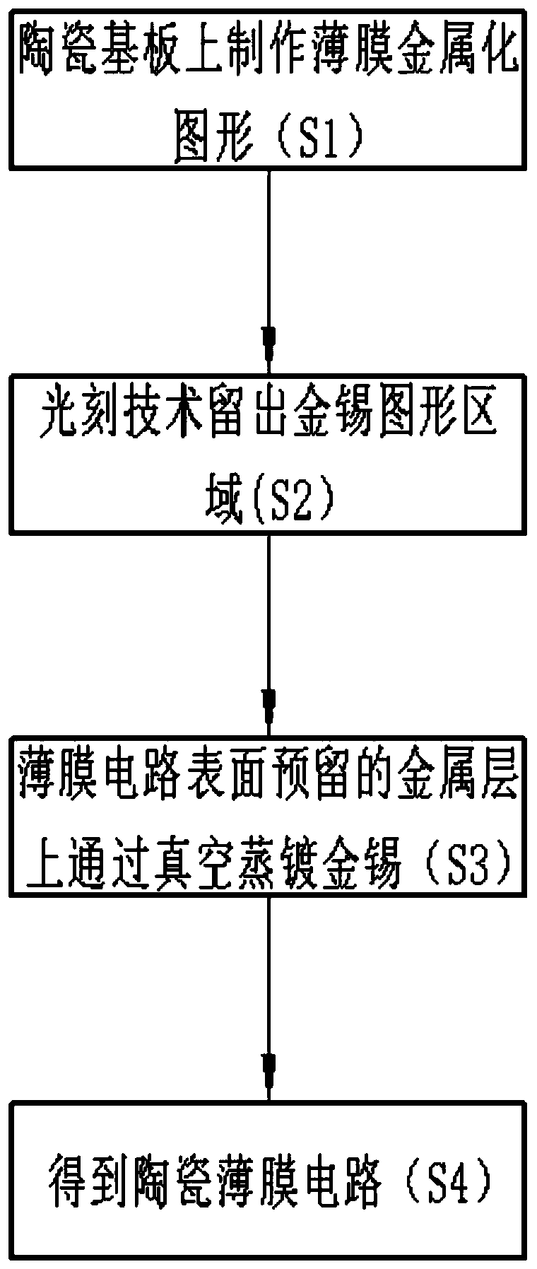
[0032] Such as figure 1 As shown, in order to achieve the technical purpose, the technical solution of the present invention is: the present invention relates to a method for selectively preparing gold-tin eutectic solder on the surface of a ceramic thin film circuit for a 5G optical module, comprising the following steps:

[0033] S1: making a thin film metallization pattern on a ceramic substrate;

[0034] S2: Leave a gold-tin pattern area by photolithography in the designated area of ​​​​the film metallization surface;

[0035] S3: Vacuum evaporation of gold and tin on the metal layer reserved on the surface ...


PUM


Abstract

The invention relates to a method for selectively preparing a gold-tin eutectic solder on the surface of a ceramic thin film circuit of a 5G optical module. Through the method, a gold-tin alloy not only has good wettability, weldability and corrosion resistance, but also has high stability. By using the gold-tin solder prepared by the method, a gold-tin plating layer with a bright and compact surface can be obtained at a specified position, the thickness of a gold layer and the thickness of a tin layer are controllable, the wettability is good after gold-tin eutectic formation, and different packaging requirements can be met. The melting point of the formed eutectic alloy is 280+ / -0.2 DEG C, and the gold-tin alloy solder can be preset on a thin film circuit. The packaging accuracy and yield are improved, and the welding requirements of small chips are met.

Description

technical field [0001] The invention relates to the field of micro ceramic products, in particular to a method for selectively preparing gold-tin eutectic solder on the surface of a ceramic thin film circuit for a 5G optical module. Background technique [0002] At present, most of the gold-tin solders on the surface of ceramics in China are deposited through gold-tin solder preforms or electroplating deposition methods, that is, electroplating. Gold-tin alloy solder has a low melting point and has no corrosion effect on the gold-plated layer of microelectronic devices. It has high joint strength, excellent corrosion resistance, high thermal conductivity and thermal shock resistance. It is a common solder for various high-reliability electronic devices. connect material. At present, the products tend to be miniaturized. Au80Sn20 in the alloy state of gold-tin solder preforms is composed of hexagonal lattice phase and intermetallic compounds, which is brittle and difficult t...

Claims


Application Information

Patent Timeline
IPC IPC(8): H05K3/34
CPCH05K3/3457H05K3/3473
Inventor 商炜于莎莎夏俊峰
Owner 苏州厚朴传感科技有限公司
Learn More