Microdefect-induced electrochromic intelligent glass composite membrane group and preparation method thereof

An electrochromic and smart glass technology, applied in the direction of ion implantation plating, coating, instruments, etc., can solve the problems of affecting the discoloration time of the material, the discoloration process is easy to be uneven, and the reaction rate is affected, so as to improve the uniformity of discoloration, Improve the color changing efficiency and speed up the coloring time

Pending Publication Date: 2020-03-31
(CNBM) BENGBU DESIGN & RES INST FOR GLASS IND CO LTD
View PDF9 Cites 2 Cited by
  • Summary
  • Abstract
  • Description
  • Claims
  • Application Information

AI Technical Summary

Problems solved by technology

For example, in the electrochromic process, the electrochromic material undergoes a redox charge transfer reaction under an applied voltage. Inside the color-changing material, the material lattice or molecular bonds will be irreversibly damaged or broken. At the same time, the interface between the electrode, electrolyte layer and electrochromic material will also directly affect the mass transfer process of the device, thereby affecting the overall reaction rate. Ultimately affects the discoloration time of the material; and because an external electric field is usually applied around the device, the discoloration process of the electrochromic device usually spreads from the surrounding to the middle, resulting in uneven electrochromic process

Method used


Image

  • Microdefect-induced electrochromic intelligent glass composite membrane group and preparation method thereof

Examples


Embodiment 1

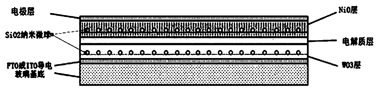
[0016] (1) Preparation of embedded SiO 2 WO of nanospheres 3 Layer: On the FTO or ITO surface of the FTO or ITO conductive glass substrate, first prepare WO with a thickness of 20nm by DC reactive magnetron sputtering 3 layer, followed by scrape coating, coating 5% solid content silicon oxide nanosphere emulsion on WO 3 layer, in WO 3 Discrete SiO 2 Microspheres, the diameter of which is 100nm; the WO with a thickness of 300nm was prepared by DC reactive magnetron sputtering again 3 layer, wherein the target material of magnetron sputtering is a metal plane tungsten target, the sputtering pressure is 0.37Pa, the sputtering power is 800W, the sputtering argon flow rate is 200sccm, and the oxygen flow rate is 55sccm;

[0017] (2) Preparation of electrolyte layer: WO prepared in step (1) 3 On the layer, a layer of Li with a thickness of 100 nm was prepared by DC reactive sputtering method. x Ga y O layer, the target used is Li, Ga alloy target, the Li / Ga mixing mass ratio ...

Embodiment 2

[0021] (1) Preparation of embedded SiO 2 WO of nanospheres 3 Layer: On the FTO or ITO surface of the FTO or ITO conductive glass substrate, first prepare WO with a thickness of 50nm by DC reactive magnetron sputtering 3 layer, followed by scrape coating, coating 5% solid content silicon oxide nanosphere emulsion on WO 3 layer, in WO 3 Discrete SiO 2 Microspheres, the diameter of the microspheres is 50nm; the WO with a thickness of 200nm is prepared by DC reactive magnetron sputtering again. 3 layer, wherein the magnetron sputtering target is a metal flat tungsten target, the sputtering pressure is 1.0Pa, the sputtering power is 1000W, the sputtering argon flow rate is 450 sccm, and the oxygen flow rate is 120 sccm;

[0022] (2) Preparation of electrolyte layer: WO prepared in step (1) 3 On the layer, a layer of Li with a thickness of 200nm was prepared by DC reactive sputtering method. x Ga y O layer, the target used is Li, Ga alloy target, the Li / Ga mixing mass ratio i...

Embodiment 3

[0026] (1) Preparation of embedded SiO 2 WO of nanospheres 3 Layer: On the FTO or ITO surface of the FTO or ITO conductive glass substrate, first prepare WO with a thickness of 90nm by DC reactive magnetron sputtering 3 layer, followed by scrape coating, coating 5% solid content silicon oxide nanosphere emulsion on WO 3 layer, in WO 3 Discrete SiO 2 Microspheres, the diameter of the microspheres is 20nm; the WO with a thickness of 150nm is prepared again by the DC reactive magnetron sputtering method 3 layer, wherein the magnetron sputtering target is a metal planar tungsten target, the sputtering pressure is 1.5Pa, the sputtering power is 1500W, the sputtering argon flow rate is 450 sccm, and the oxygen flow rate is 50 sccm;

[0027] (2) Preparation of electrolyte layer: WO prepared in step (1) 3 On the layer, a layer of Li with a thickness of 300nm was prepared by DC reactive sputtering method. x Nb y O layer, the targets used are Li and Nb alloy targets, the Li / Ga mi...


PUM

PropertyMeasurementUnit
thicknessaaaaaaaaaa
thicknessaaaaaaaaaa
thicknessaaaaaaaaaa

Abstract

The invention relates to a microdefect-induced electrochromic intelligent glass composite film group and a preparation method thereof. The microdefect-induced electrochromic intelligent glass composite film group is characterized in that a WO3 layer, an electrolyte layer, a NiO layer and an electrode layer are sequentially arranged on an FTO or ITO surface of an FTO or ITO conductive glass substrate, wherein SiO2 nano microspheres are embedded in the WO3 layer and the NiO layer, the electrolyte layer is a Li < x > Ga < y > O or Li < x > Nb < y > O layer, and the electrode layer is an ITO layer. The beneficial effects of the invention are that: SiO2 nano particles are embedded in the color-changing layer to serve as micro defects; the micro-defect nanospheres and the color-changing layer can form interface defects to promote induced aggregation of ions at a micro-defect interface in the electrochromism process, so that the purpose of improving the color-changing efficiency of the film is achieved, including accelerating the coloring time, increasing the light modulation amplitude, improving the color-changing uniformity and the like. According to the method for preparing the ITO electrode layer through normal-temperature sputtering, the ITO thin film is prepared through normal-temperature sputtering, the performance of the thin film is guaranteed, and meanwhile possible influences of heating on a film system color changing layer and an electrolyte layer are avoided.

Description

technical field [0001] The present invention relates to a kind of preparation method of electrochromic film group, specifically a kind of nano-SiO 2 An ion-induced electrochromic smart glass composite membrane group and a preparation method thereof generated by particles as a micro-defect embedded color-changing layer. Background technique [0002] At present, our world is entering the era of intelligence at an unprecedented speed. Under such an era background, the field of material research has also set off an upsurge of intelligence. Smart materials represent the direction of future material research. Among them, electrochromic materials are a kind of in many fields. Smart materials with great potential and advantages. Electrochromism means that the optical properties (transmission, reflection, absorption, etc.) of materials can produce stable and reversible changes under the action of an applied electric field or current. As a new type of smart material, electrochromic ...

Claims


Application Information

Patent Timeline
Patent Type & Authority Applications(China)
IPC IPC(8): G02F1/1524C23C14/08C23C14/35C23C14/34
CPCG02F1/1524G02F1/1525C23C14/083C23C14/35C23C14/0036C23C14/08C23C14/085C23C14/34
Inventor 彭寿汤永康马立云甘治平李刚沈洪雪金克武张道清王家勇
Owner (CNBM) BENGBU DESIGN & RES INST FOR GLASS IND CO LTD
Why Eureka
Try Eureka