Nickel oxide film and preparation method thereof, and quantum dot light emitting diode
A technology of quantum dot luminescence and nickel oxide film, applied in electrical components, circuits, semiconductor devices, etc., can solve problems such as unfavorable hole injection and limitation, reduce and non-radiative recombination centers, facilitate deposition, and improve luminous efficiency Effect
- Summary
- Abstract
- Description
- Claims
- Application Information
AI Technical Summary
Problems solved by technology
Method used
Image

Examples
Embodiment 1
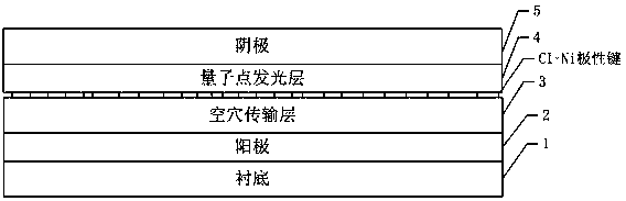
[0054] A quantum dot light-emitting diode, which includes an anode, a hole transport layer, a quantum dot light-emitting layer, an electron transport layer, and a cathode that are sequentially stacked from bottom to top, and its specific preparation includes the following steps:
[0055] 1. Use transparent conductive film ITO as the anode with a thickness of 50nm;
[0056] 2. Deposit a NiO film on the anode by magnetron sputtering, with a thickness of 30nm;
[0057] 3. Drop o-dichlorobenzene on the surface of the NiO film layer and make the o-dichlorobenzene cover the surface of the NiO film layer, and then carry out under the condition that the UV light power is 80W and the UV light time is 3min. Carrying out ultraviolet light to grow Cl-Ni polar bonds on the surface of the NiO film layer to prepare a nickel oxide film, and use the nickel oxide film as a hole transport layer;
[0058] 4. Deposit CdSe / ZnS on the hole transport layer as a quantum dot light-emitting layer by so...
Embodiment 2
[0062] A quantum dot light-emitting diode, which includes an anode, a hole transport layer, a quantum dot light-emitting layer, an electron transport layer, and a cathode that are sequentially stacked from bottom to top, and its specific preparation includes the following steps:
[0063] 1. Use transparent conductive film ITO as the anode with a thickness of 50nm;
[0064] 2. Deposit a NiO film on the anode by magnetron sputtering, with a thickness of 30nm;
[0065] 3. Add chlorobenzene dropwise on the surface of the NiO film and make the chlorobenzene cover the surface of the NiO film, and then carry out ultraviolet light under the condition that the UV light power is 150W and the UV light time is 5min. Illumination, so that Cl-Ni polar bonds are grown on the surface of the NiO film layer, and a nickel oxide film is obtained, and the nickel oxide film is used as a hole transport layer;
[0066] 4. Deposit CdSe / ZnS on the hole transport layer as a quantum dot light-emitting l...
Embodiment 3
[0070]A quantum dot light-emitting diode, which includes an anode, a hole transport layer, a quantum dot light-emitting layer, an electron transport layer, and a cathode that are sequentially stacked from bottom to top, and its specific preparation includes the following steps:
[0071] 1. Use transparent conductive film ITO as the anode with a thickness of 50nm;
[0072] 2. Deposit a NiO film on the anode by magnetron sputtering, with a thickness of 30nm;
[0073] 3. Add chloroform dropwise on the surface of the NiO film layer and make the chloroform cover the surface of the NiO film layer, and then carry out ultraviolet light irradiation in an ozone environment under the condition that the ultraviolet light power is 200W and the ultraviolet light time is 10min. growing Cl-Ni polar bonds on the surface of the NiO film layer to prepare a nickel oxide film, using the nickel oxide film as a hole transport layer;
[0074] 4. Deposit CdSe / ZnS as the quantum dot light-emitting lay...
PUM
| Property | Measurement | Unit |
|---|---|---|
| thickness | aaaaa | aaaaa |
| thickness | aaaaa | aaaaa |
| thickness | aaaaa | aaaaa |
Abstract
Description
Claims
Application Information
 - R&D
- Intellectual Property
- Life Sciences
- Materials
- Tech Scout
- Unparalleled Data Quality
- Higher Quality Content
- 60% Fewer Hallucinations
Browse by: Latest US Patents, China's latest patents, Technical Efficacy Thesaurus, Application Domain, Technology Topic, Popular Technical Reports.
© 2025 PatSnap. All rights reserved.Legal|Privacy policy|Modern Slavery Act Transparency Statement|Sitemap|About US| Contact US: help@patsnap.com