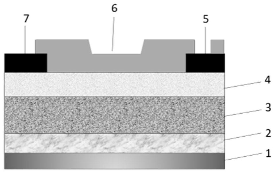
A kind of gan rectifier based on cu substrate and preparation method thereof
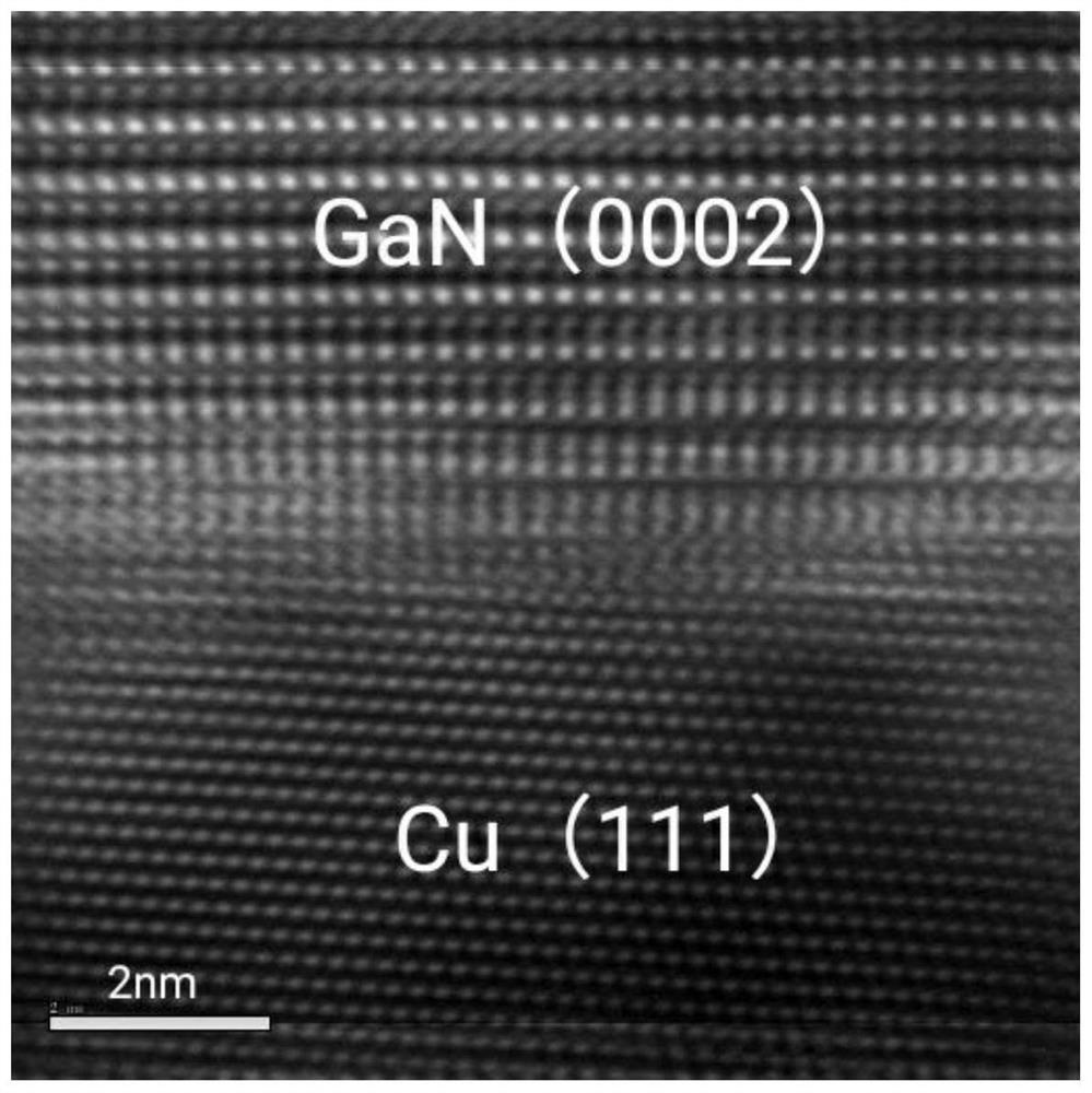
A rectifier and substrate technology, applied in the field of Cu-substrate-based GaN rectifier and its preparation, achieves the effects of stable performance, clear hetero interface and excellent crystal quality
- Summary
- Abstract
- Description
- Claims
- Application Information
AI Technical Summary
Problems solved by technology
Method used
Image
Examples
Embodiment 1
[0029] A method for preparing a GaN rectifier based on a Cu substrate, comprising the steps of:
[0030] S1 At room temperature, the single crystal Cu(111) substrate was cleaned and dried, then placed in a rapid annealing furnace, fed with 30 sccm argon, and annealed at 400°C to obtain a clean single crystal Cu substrate, and sent to In a pulsed laser deposition (PLD) chamber;
[0031] S2 uses the general process method of electron beam evaporation to selectively deposit a 5 μm graphite layer on a 2-inch GaN target. The target area covered by the graphite layer and the target area not covered by the graphite layer are distributed axisymmetrically, and the area ratio is 2. .
[0032] S3 uses the method of pulsed laser deposition (PLD), setting the energy of the PLD laser to 380mJ, the frequency at 20Hz, the growth temperature at 600°C, the distance between the target and the substrate at 4mm, and the cavity pressure at 4mTorr. 111) A 2μm carbon-doped GaN high-resistance layer...
Embodiment 2
[0038] A method for preparing a GaN rectifier based on a Cu substrate, comprising the steps of:
[0039] S1 At room temperature, the single crystal Cu(111) substrate was cleaned and dried, then placed in a rapid annealing furnace, fed with 30 sccm argon, and annealed at 400°C to obtain a clean single crystal Cu substrate, and sent to In a pulsed laser deposition (PLD) chamber;
[0040] S2 uses the general process method of electron beam evaporation to selectively deposit a 6 μm graphite layer on a 2-inch GaN target. The target area covered by the graphite layer and the target area not covered by the graphite layer are distributed axisymmetrically, and the area ratio is 2. .
[0041] S3 Through the general process method of pulsed laser deposition (PLD), set the energy of the PLD laser to 400mJ, maintain the frequency at 25Hz, maintain the growth temperature at 640°C, maintain the distance between the target and the substrate at 4.5mm, and maintain the cavity pressure at 4.5mT...
Embodiment 3
[0047] A method for preparing a GaN rectifier based on a Cu substrate, comprising the steps of:
[0048] S1 At room temperature, the single crystal Cu(111) substrate was cleaned and dried, then placed in a rapid annealing furnace, fed with 30 sccm argon, and annealed at 400°C to obtain a clean single crystal Cu substrate, and sent to In a pulsed laser deposition (PLD) chamber;
[0049] S2 uses the general process method of electron beam evaporation to selectively deposit a 4.5 μm graphite layer on a 2-inch GaN target. The target area covered by the graphite layer and the target area not covered by the graphite layer are distributed axisymmetrically, and the area ratio is 2.
[0050] S3 Through the general process method of pulsed laser deposition (PLD), set the PLD laser energy to 350mJ, maintain the frequency at 30Hz, maintain the growth temperature at 680°C, maintain the distance between the target and the substrate at 5mm, and maintain the cavity pressure at 5mTorr. A 2μm...
PUM
| Property | Measurement | Unit |
|---|---|---|
| thickness | aaaaa | aaaaa |
| thickness | aaaaa | aaaaa |
| thickness | aaaaa | aaaaa |
Abstract
Description
Claims
Application Information

