
Hot isostatic pressing crystal growth device

A technology of crystal growth and hot isostatic pressing, applied in the direction of crystal growth, single crystal growth, single crystal growth, etc., can solve problems such as corrosion

Inactive Publication Date: 2020-04-17
SHANGHAI XITANG SEMICON TECH CO LTD
View PDF7 Cites 0 Cited by
  • Summary
  • Abstract
  • Description
  • Claims
  • Application Information

AI Technical Summary

Problems solved by technology

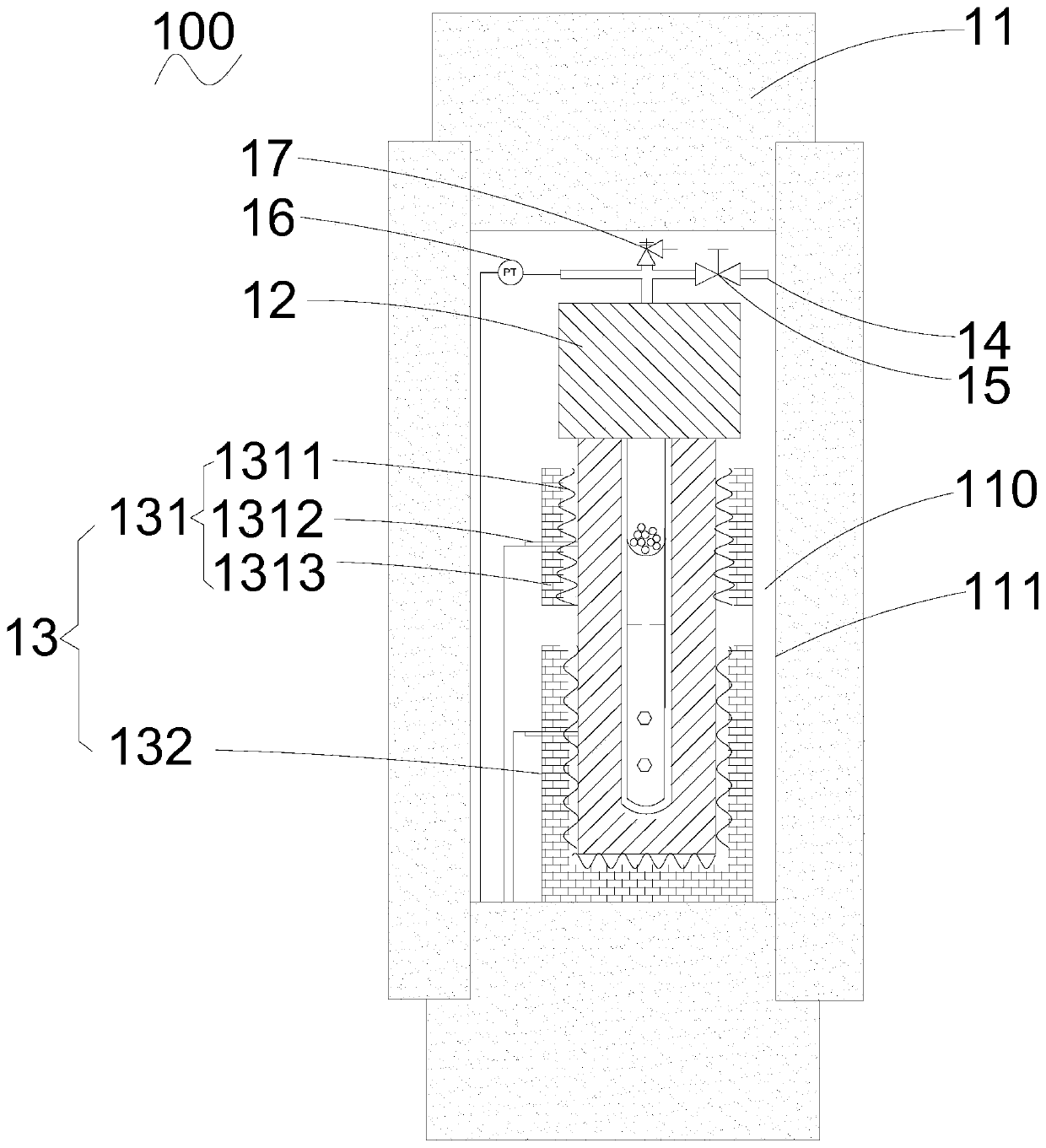
[0004] Based on this, it is necessary to provide an improved hot isostatic pressing crystal growth device for the problem that the leakage of supercritical ammonia is easy to cause corrosion on the inner wall of the hot isostatic pressing device

Method used


Image

  • Hot isostatic pressing crystal growth device
  • Hot isostatic pressing crystal growth device

Examples


Embodiment Construction

[0020] In order to facilitate the understanding of the present invention, the present invention will be described more fully below with reference to the relevant drawings. The preferred embodiments of the present invention are shown in the drawings. However, the present invention can be implemented in many different forms and is not limited to the embodiments described herein. On the contrary, the purpose of providing these embodiments is for a more thorough and comprehensive understanding of the disclosure of the present invention.

[0021] It should be noted that when an element is referred to as being "fixed to" another element, it can be directly on the other element or a central element may also exist. When an element is considered to be "connected" to another element, it can be directly connected to the other element or an intermediate element may be present at the same time. The terms "vertical", "horizontal", "left", "right", "upper", "lower", "front", "rear", "circumfe...


PUM


Abstract

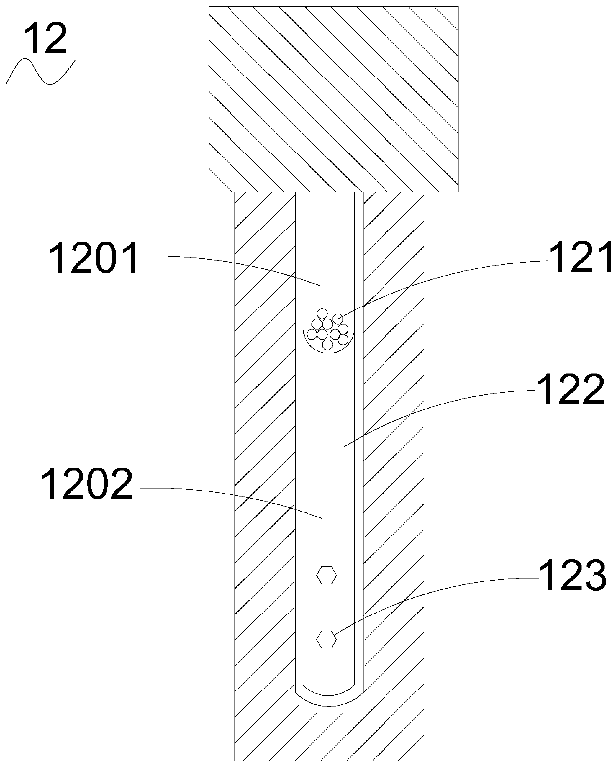
The invention relates to a hot isostatic pressing crystal growth device which comprises a first container, wherein at least one second container is contained in an inner cavity of the first container,the second container is used for containing raw materials, mineralizers and seed crystals, a heating part is arranged between the outer wall of the second container and the inner wall of the first container, and the part, exposed out of the inner cavity of the first container, of the inner wall of the first container is covered with an anti-corrosion coating. The hot isostatic pressing crystal growth device can effectively prevent corrosive substances in the second container from corroding the inner wall of the first container when leaking, so that the maintenance cost of the device is reduced, the later maintenance of the device is facilitated, and the growth period of crystals is guaranteed.

Description

Technical field [0001] The invention relates to the technical field of semiconductor materials, in particular to a hot isostatic pressing crystal growth device. Background technique [0002] The third-generation semiconductor material is a wide-gap semiconductor material represented by gallium nitride (GaN), silicon carbide (SiC), diamond, and zinc oxide. Its band gap energy can reach 3.3 ~ 5.5 eV, which is different from the traditional first-generation semiconductor material. Compared with semiconductor materials silicon (Si) and germanium (Ge), second-generation semiconductor materials gallium arsenide (GaAs) and indium phosphide (InP), the third-generation semiconductor materials have a large band gap, high breakdown electric field, The unique properties of high thermal conductivity, high electronic saturation drift speed, low dielectric constant, etc., make it show great application potential in optoelectronic devices, power electronics, radio frequency microwave devices, la...

Claims


Application Information

Patent Timeline
IPC IPC(8): C30B35/00C30B29/40
CPCC30B29/406C30B35/00
Inventor 乔焜高明哲林岳明
Owner SHANGHAI XITANG SEMICON TECH CO LTD
Learn More