
Method for measuring and calculating doping concentration of highly-doped semiconductor

A technology of doping concentration and semiconductor, which is applied in measurement devices, instruments, material analysis by electromagnetic means, etc., can solve problems such as the inability to accurately reflect the actual doping concentration of semiconductor materials, and achieve improved ohmic contact efficiency and high accuracy. Effect

Pending Publication Date: 2020-04-17
SOUTH UNIVERSITY OF SCIENCE AND TECHNOLOGY OF CHINA
View PDF5 Cites 1 Cited by
  • Summary
  • Abstract
  • Description
  • Claims
  • Application Information

AI Technical Summary

Problems solved by technology

The four-probe method is often used to test the resistivity of semiconductor materials. According to the conductivity formula, the result of the four-probe method is the product of the carrier concentration and mobility in the semiconductor material. Since the mobility is affected by scattering, the Doping concentration and temperature change, while the carrier concentration is only the same as the actual doping concentration in the semiconductor under strong ionization, so this method cannot accurately reflect the actual doping concentration of the semiconductor material

Method used


Image

  • Method for measuring and calculating doping concentration of highly-doped semiconductor
  • Method for measuring and calculating doping concentration of highly-doped semiconductor
  • Method for measuring and calculating doping concentration of highly-doped semiconductor

Examples


Embodiment 1

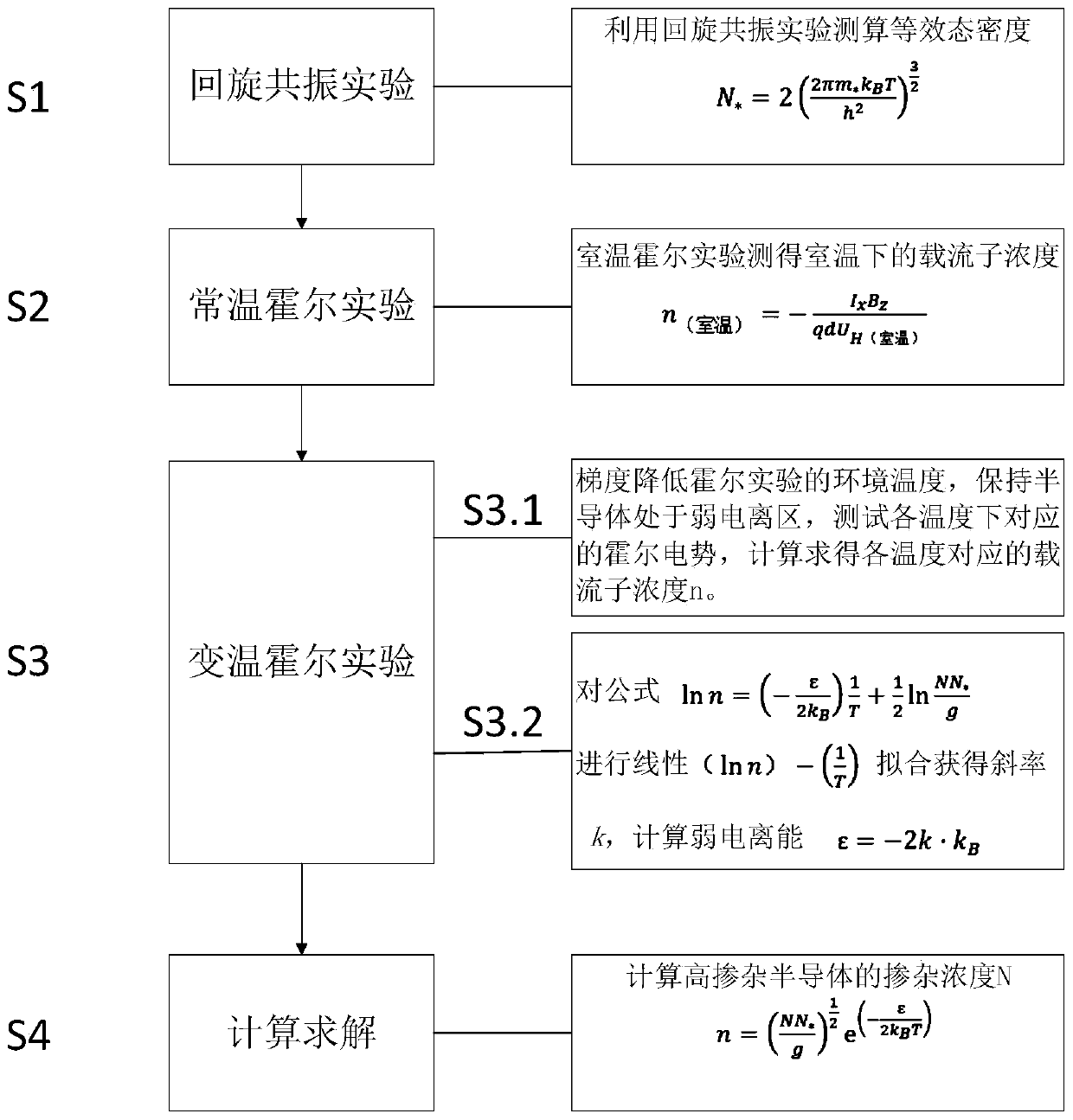
[0030] This embodiment provides a method for calculating the doping concentration of N-type highly doped silicon carbide, such as figure 1 As shown, the steps of the method include:

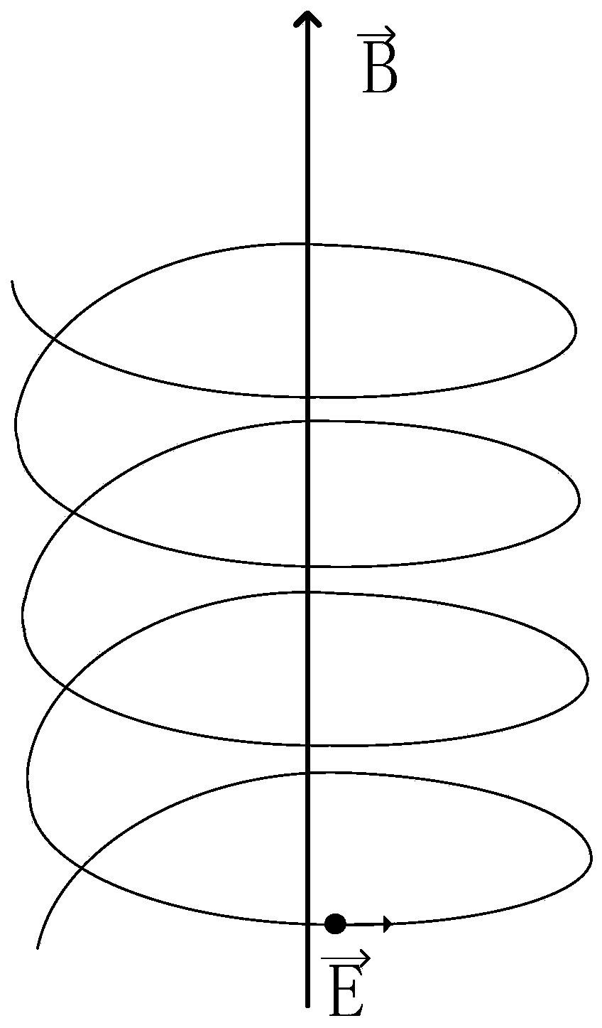
[0031] S1. Obtain the conduction band equivalent density of states N by cyclotron resonance experiment C ,Such as figure 2 As shown, the specific experimental steps of the cyclotron resonance test are: add a constant magnetic field B to the silicon carbide sample, and then apply an alternating electromagnetic field, and let the electric component E be perpendicular to the constant magnetic field B. Due to the effect of the Lorentz force, the electrons in the semiconductor do spiral motion around the magnetic field on the one hand, and are also affected by the alternating electromagnetic field on the other hand. When the frequency ω of the electromagnetic field and the cyclotron frequency of the electron At the same time, electrons will be continuously accelerated by the alternating electromag...

Embodiment 2

[0039] This embodiment provides a method for calculating the doping concentration of P-type highly doped gallium nitride, including:

[0040] S1. Using the cyclotron resonance experiment to measure the equivalent density of states in the valence band, the cyclotron resonance experiment specifically adds a constant magnetic field B to the gallium nitride sample, and then applies an alternating electromagnetic field, and makes the electric component E perpendicular to the constant magnetic field B. Then the holes in the semiconductor do spiral motion around the magnetic field on the one hand, and are also affected by the alternating electromagnetic field on the other hand. When the frequency ω of the electromagnetic field and the cyclotron frequency of the holes At the same time, the holes will be continuously accelerated by the alternating electromagnetic field, thereby gaining energy and causing resonance absorption. By measuring the electromagnetic field frequency ω and the ...


PUM


Abstract

The invention belongs to the field of semiconductor materials and process testing, and discloses a method for measuring and calculating the doping concentration of a highly-doped semiconductor. The method at least comprises the implementation steps of S1, measuring and calculating the equivalent state density N* by utilizing a cyclotron resonance experiment; S2, measuring the carrier concentrationn(room temperature) at the room temperature through a room temperature Hall experiment; S3, calculating the weak ionization energy [epsilon] of carriers in a weak ionization region through a variabletemperature Hall experiment; and S4, calculating the doping concentration N of the highly-doped semiconductor by combining the equivalent state density N*, the carrier concentration n(room temperature) and the weak ionization energy [epsilon] obtained in the above steps. According to the method, the limitation of several existing semiconductor doping concentration testing methods is overcome, andthe doping concentration in a highly-doped semiconductor, especially in a wide bandgap semiconductor, can be obtained simply, conveniently and accurately through basic experiments and simple calculation and fitting.

Description

technical field [0001] The invention belongs to the field of semiconductor materials and process testing, in particular to a method for measuring and calculating the doping concentration of highly doped semiconductors. Background technique [0002] As an important branch of the field of microelectronic devices, discrete devices are widely used in military, aerospace, transportation and power transmission, and have a profound impact on people's production and lifestyle. The performance of semiconductor devices is closely related to the materials they use. The third-generation semiconductor materials, mainly silicon carbide and gallium nitride, have received more and more attention. Silicon carbide has excellent characteristics such as high thermal conductivity, high electron saturation rate and high radiation resistance, and is suitable for making high-temperature, high-frequency, radiation-resistant and high-power devices; gallium nitride has higher breakdown field strength ...

Claims


Application Information

Patent Timeline
Patent Type & Authority Applications(China)
IPC IPC(8): G01N24/14G01N27/00
CPCG01N24/14G01N27/00
Inventor 陈施施张新河温正欣叶怀宇张国旗
Owner SOUTH UNIVERSITY OF SCIENCE AND TECHNOLOGY OF CHINA
Learn More