

P-type single crystal PERC battery capable of improving LeTID phenomenon and manufacturing method thereof
A production method and single crystal technology, applied in sustainable manufacturing/processing, circuits, photovoltaic power generation, etc., can solve the problems that do not conform to the development trend of cost reduction and efficiency improvement in the photovoltaic industry, the decline in the efficiency of batteries and modules, and excess hydrogen atoms in batteries, etc. Problems, to achieve good field passivation effect, reduce the amount of use, reduce the effect of excess hydrogen atom content
- Summary
- Abstract
- Description
- Claims
- Application Information
AI Technical Summary
Problems solved by technology
Method used
Image

Examples
Embodiment 1
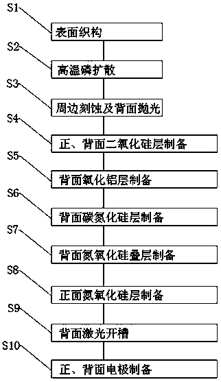
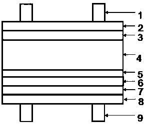
[0033] Step S1, surface texture, also known as alkali texturing, is to use alkali solution to corrode the silicon wafer substrate 4, and form a pyramid-shaped surface morphology on the surface of the silicon wafer substrate 4, wherein, the reaction alkali solution: 1.2wt% NaOH, reaction time: 400s, temperature: 80°C, reflectance after treatment: 11%;
[0034] Step S2, high-temperature phosphorus diffusion, nitrogen gas is passed through a constant temperature liquid source bottle, and the diffusion source phosphorus oxychloride is brought into a high-temperature diffusion furnace, and a sufficient amount of oxygen is introduced at the same time, after the reaction, phosphorus atoms diffuse into the interior of the P-type silicon wafer , forming an N-type impurity distribution, and obtaining a PN junction, wherein, nitrogen flow rate: 700sccm, oxygen flow rate: 800sccm, reaction time: 88min, temperature: 800°C, diffusion resistance: 120 ohms; and then laser doping method is form...
Embodiment 2
[0044] Step S1, surface texture, also known as alkali texturing, that is, using an alkali solution to corrode the silicon wafer substrate, forming a pyramid-shaped surface morphology on the surface of the silicon wafer substrate, wherein the reaction alkali solution: 1.2wt% NaOH, Reaction time: 400s, temperature: 80°C, reflectivity after treatment: 11%;
[0045] Step S2, high-temperature phosphorus diffusion, wherein, nitrogen flow rate: 700sccm, oxygen flow rate: 800sccm, reaction time: 88min, temperature: 800°C, diffusion resistance: 120 ohms; and then laser doping method to form a heavily doped region in the front electrode region, Square resistance: 95 ohms;
[0046] Step S3, peripheral etching and back polishing, using 49% HF acid solution to etch the back and edge of the silicon wafer diffused in step 2, and then using 45% KOH and polishing additives to polish the back of the silicon wafer Processing, weight reduction: 0.25g, back reflectivity: 42%;
[0047] Step S4, s...
PUM
| Property | Measurement | Unit |
|---|---|---|
| Thickness | aaaaa | aaaaa |
| Thickness | aaaaa | aaaaa |
| Thickness | aaaaa | aaaaa |
Abstract
Description
Claims
Application Information