Method for adjusting synaptic plasticity of metal oxide synaptic transistor

A technology of oxides and transistors, applied in semiconductor devices, semiconductor/solid-state device manufacturing, electrical components, etc., can solve the problems of difficulty in controlling the accuracy of synapse weight adjustment, long device preparation time, and complicated preparation processes, etc., to achieve improved synapse Touch performance, low cost, simple operation

Active Publication Date: 2020-04-21
FUZHOU UNIV
View PDF5 Cites 3 Cited by
  • Summary
  • Abstract
  • Description
  • Claims
  • Application Information

AI Technical Summary

Problems solved by technology

[0003] The adjustment of synaptic plasticity (that is, synaptic weight) is the key to simulating the biological nervous system. The traditional way of adjusting synaptic weight is mainly through the design of materials and the

Method used


Image

  • Method for adjusting synaptic plasticity of metal oxide synaptic transistor
  • Method for adjusting synaptic plasticity of metal oxide synaptic transistor

Examples


Embodiment 1

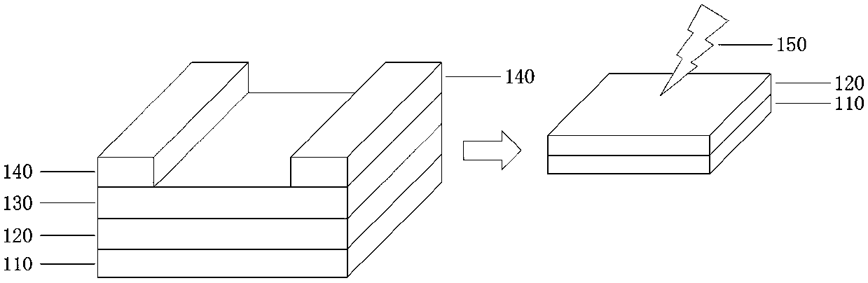
[0031] 1) A pure silicon wafer with a size of 1.5 cm×1.5 cm was ultrasonically cleaned with acetone, isopropanol, and deionized water, and then washed with deionized water and dried with nitrogen to obtain a clean silicon wafer as a substrate.

[0032] 2) Put Ta 2 o 5 Sputter on the silicon wafer in step 1) as an insulating layer, the sputtering power is 100 W, the pressure is 0.35 Pa, the rotation speed is 250 R, the argon-oxygen ratio is set to 30:2.5, the sputtering time is 14 minutes, and the thickness is about 120 nm.

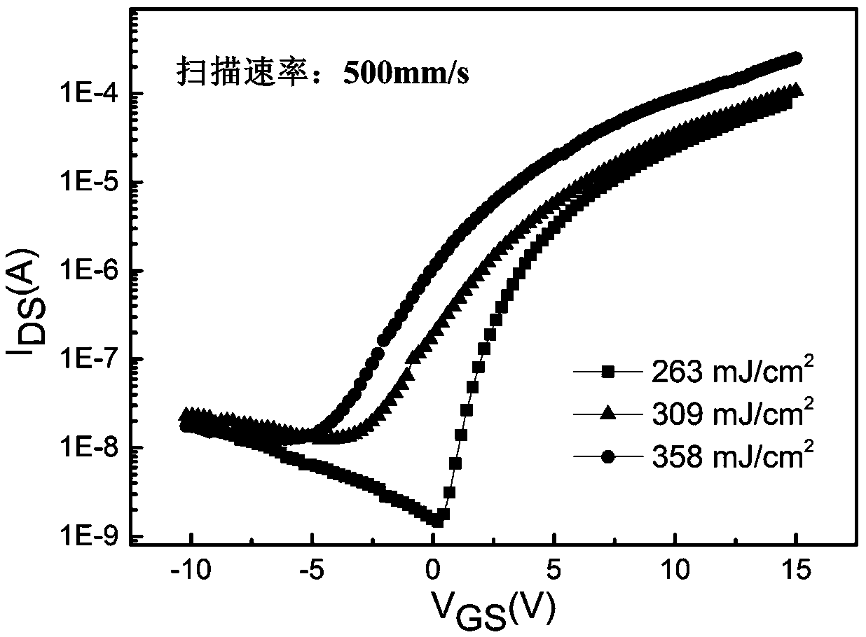
[0033] 3) The Ta obtained in step 2) 2 o 5 The thin film is processed by laser. The selected laser has a wavelength of 517 nm, a pulse output, a repetition frequency of 1 MHz, and a pulse width of 283 fs. The laser scanning method is set to grid scanning, the laser scanning rate is set to 500mm / s, and the laser power can be selected from 0 to 400 mJ / cm 2 between. The obtained transfer characteristic curve is as follows figure 2 shown.

[0034] 4) ...

Embodiment 2

[0037] 1) A pure silicon wafer with a size of 1.5 cm×1.5 cm was ultrasonically cleaned with acetone, isopropanol, and deionized water, and then washed with deionized water and dried with nitrogen to obtain a clean silicon wafer as a substrate.

[0038] 2) Put Ta 2 o 5 Sputter on the silicon wafer in step 1) as an insulating layer, the sputtering power is 100 W, the pressure is 0.35 Pa, the rotation speed is 250 R, the argon-oxygen ratio is set to 30:2.5, the sputtering time is 14 minutes, and the thickness is about 120 nm.

[0039] 3) The Ta obtained in step 2) 2 o 5 The thin film is processed by laser. The selected laser has a wavelength of 517 nm, a pulse output, a repetition frequency of 1 MHz, and a pulse width of 283 fs. The laser scanning method is set to grid scanning, and the laser power is set to 300 mJ / cm 2 , the laser scanning speed can be selected between 300~700 mm / s.

[0040] 4) Sputter the semiconductor layer indium tin oxide on the silicon wafer in step 3) ...


PUM


Abstract

The invention relates to a method for adjusting the synaptic plasticity of a metal oxide synaptic transistor. The metal oxide synapse transistor is of a bottom gate top contact structure and comprisesa substrate, an insulating layer, an active layer, a source electrode and a drain electrode which are sequentially arranged from bottom to top; after the insulating layer of the metal oxide synaptictransistor is prepared, laser irradiation treatment is conducted; and the synaptic response characteristic of the metal oxide synaptic transistor is adjusted by adjusting laser irradiation parameters.The method is beneficial for quickly and conveniently adjusting the synaptic plasticity of the synaptic transistor at low temperature.

Description

technical field [0001] The invention belongs to the technical field of electronic materials and devices, and in particular relates to a method for regulating synaptic plasticity of metal oxide synaptic transistors. Background technique [0002] A metal oxide synaptic transistor is a three-terminal synaptic transistor made of metal oxide semiconductor materials. Compared with traditional two-terminal synaptic devices such as memristors, phase-change memories, and atomic switches, three-terminal metal oxide synaptic transistors have the advantages of low power consumption, high integration, and similarity to biological neural architectures. Among them, synaptic transistor devices based on solid electrolytes have great development potential due to their good environmental stability and electrical performance. [0003] The adjustment of synaptic plasticity (that is, synaptic weight) is the key to simulating the biological nervous system. The traditional way of adjusting synapti...

Claims


Application Information

Patent Timeline
IPC IPC(8): H01L29/06H01L21/336H01L29/78
CPCH01L29/0603H01L29/66969H01L29/78
Inventor 陈惠鹏杨倩陈耿旭郭太良吕东旭黄金松
Owner FUZHOU UNIV
Why Eureka
Try Eureka