

Preparation method and application of transparent conductive oxide film
An oxide thin film, transparent and conductive technology, which is applied in the direction of circuits, electrical components, semiconductor devices, etc., can solve the problems of limited carrier mobility improvement ability, high preparation cost, and increased process complexity, so as to improve the carrier Mobility, carrier mobility improvement, and the effect of increasing short-circuit current density
- Summary
- Abstract
- Description
- Claims
- Application Information
AI Technical Summary
Problems solved by technology
Method used
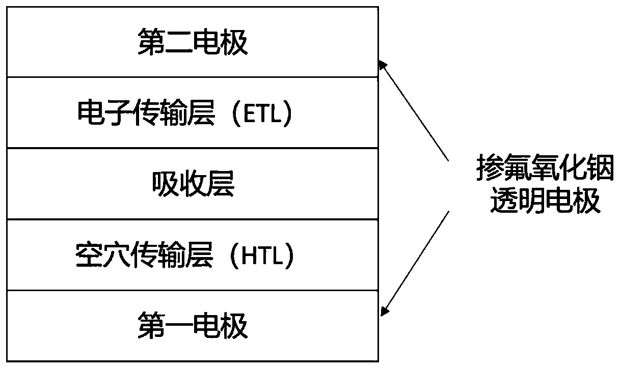
Image

Examples
Embodiment 1
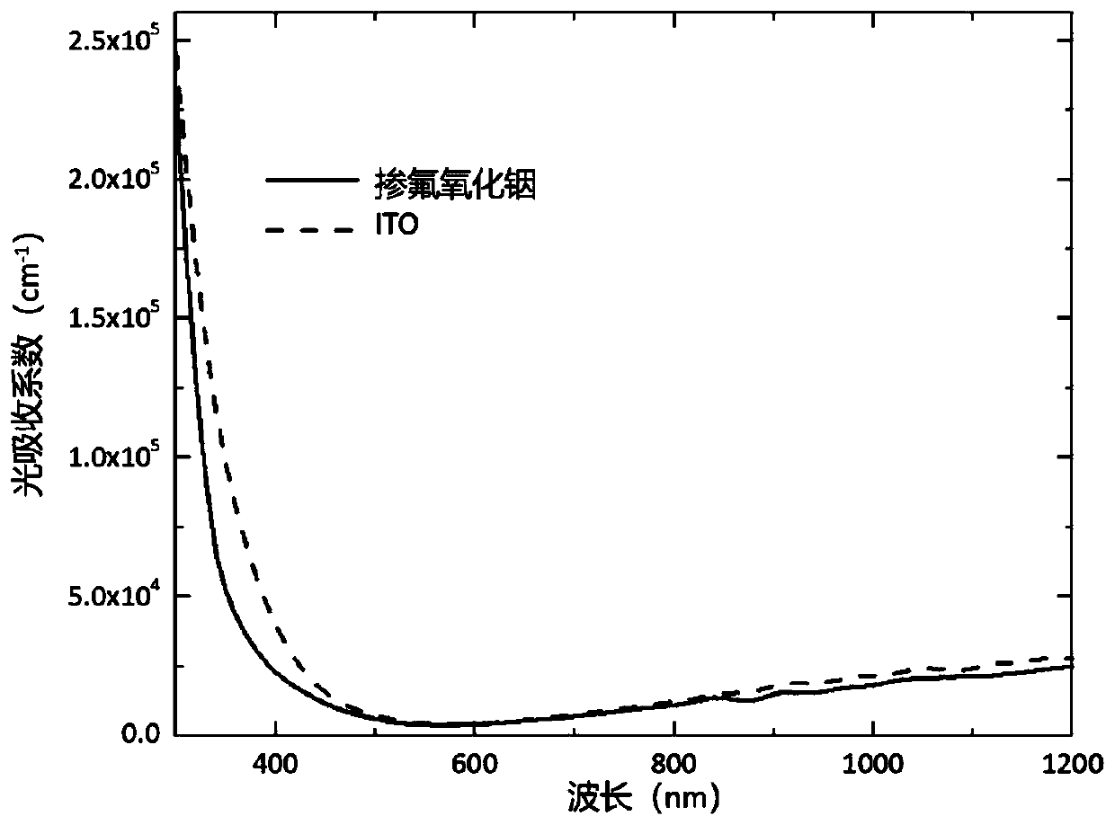
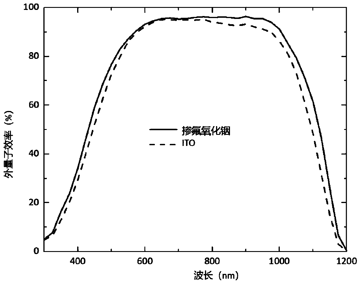
[0048] Example 1: Add argon into the chamber, use RF magnetron sputtering deposition, use fluorine-doped indium oxide as the target, the fluorine / indium atomic ratio in the target is 17%, the argon flow rate is 50sccm, and the deposition temperature is 100℃ , Deposition pressure 1.0×10 -4 Pa, deposition power density 1.8W / cm 2 . A film of 75nm thickness is deposited on the surface of Corning glass. For comparison, take In 2 O 3 :SnO 2 = 9:1 target, for sputtering deposition of conventional ITO film, ITO film thickness is 75nm.
[0049] Perform EDAX energy spectrum analysis on the prepared fluorine-doped indium oxide film to analyze the proportion of doping elements; perform Hall test and UV-Vis-IR test on the fluorine-doped indium oxide film and ITO respectively to evaluate the electrical and optical properties of the comparative film performance. The test results show that in the prepared fluorine-doped indium oxide, the fluorine / indium atomic ratio is -17%, and the carrier mo...
Embodiment 2
[0050] Example 2: Add argon and hydrogen into the chamber, use RF magnetron sputtering deposition, use fluorine-doped indium oxide as the target, the fluorine / indium atomic ratio in the target is 10%, the argon flow rate is 100 sccm, and the hydrogen gas is 2 sccm , Deposition temperature 120℃, deposition pressure 5.0×10 -4 Pa, deposition power density 0.5W / cm 2 . A 100nm thick film was deposited on the surface of Corning Glass for elemental analysis and electrical performance testing.
[0051] The results show that the fluorine / indium atomic ratio is ~10%, and its carrier mobility is 86cm 2 V -1 s -1 , The resistivity is 5.8×10 -4 Ωcm.
Embodiment 3
[0052] Example 3: Add argon and water vapor into the chamber, and deposit by DC magnetron sputtering, using fluorine-doped indium oxide as the target, the fluorine / indium atomic ratio in the target is 25%, and the argon flow rate is 100sccm. Temperature 25℃, deposition pressure 1.0×10 -2 , Water vapor partial pressure 5.0×10 -4 Pa, deposition power density 3W / cm 2 . A film with a thickness of 100nm was deposited on the surface of Corning glass, and then annealed at 450°C for 10 minutes in a nitrogen atmosphere for elemental analysis and electrical performance testing.
[0053] The results show that the fluorine / indium atomic ratio is ~25%, and the carrier mobility is 131cm 2 V -1 s -1 , The resistivity is 2.6×10 -4 Ωcm.
PUM
 Abstract
Description
Claims
Application Information