Method for prolonging carrier lifetime of silicon carbide epitaxial wafer
A technology of carrier life and epitaxial wafers, which is applied in the manufacture of electrical components, circuits, semiconductors/solid-state devices, etc., can solve the problems of inability to realize conductance modulation and low carrier life, and achieve the elimination of carbon vacancy defects and high promotion Value, the effect of simple operation
- Summary
- Abstract
- Description
- Claims
- Application Information
AI Technical Summary
Problems solved by technology
Method used
Image


Examples
Embodiment 1
[0024] A method for improving the carrier lifetime of a silicon carbide epitaxial wafer, comprising the following steps:
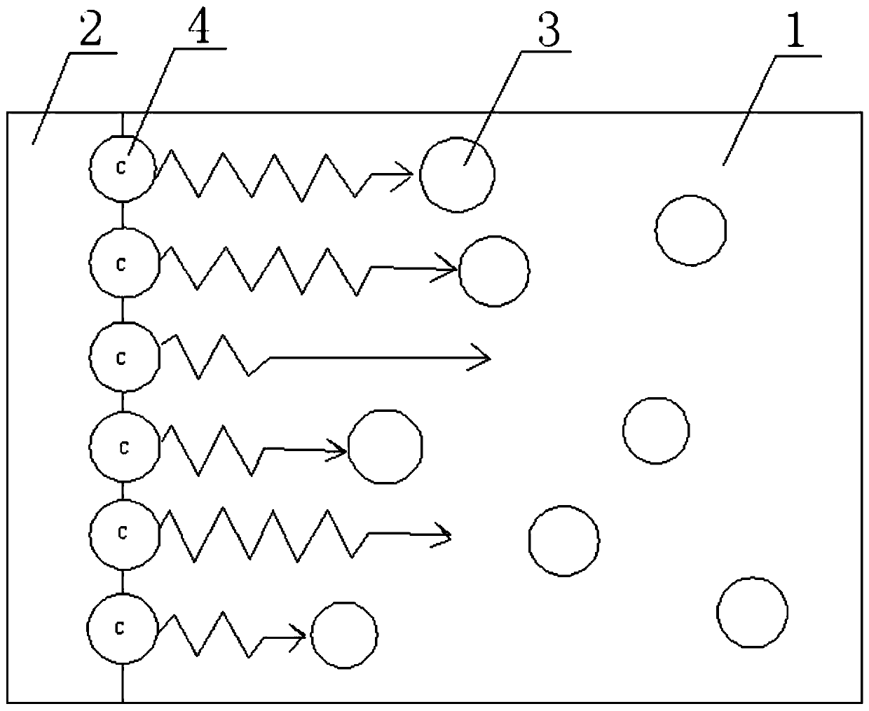
[0025] a. Preparation of silicon carbide epitaxial wafer 1: select a 4-inch silicon carbide epitaxial wafer 1 with a silicon surface at 4° to the direction, and the impurity concentration of the epitaxial layer is 5×10 14 cm -3 , the thickness of the epitaxial layer is 100 μm, and it is used after standard RCA cleaning; the carrier lifetime of the silicon carbide epitaxial wafer 1 is measured to be 1 μs by using the μ-PCD method;
[0026] b. Deposit carbon atom layer 2 on the surface: deposit carbon atom layer 2 on the surface of silicon carbide epitaxial wafer 1 by chemical vapor deposition, the deposition growth temperature is 1300°C, the carbon growth source is methane, the methane flow rate is 100 sccm, and the carbon atoms are controlled The deposition thickness of layer 2 is 100nm;
[0027] c annealing: perform annealing treatment on the silicon c...
Embodiment 2
[0030] A method for improving the carrier lifetime of a silicon carbide epitaxial wafer, comprising the following steps:
[0031] a. Preparation of silicon carbide epitaxial wafer 1: select a 4-inch silicon carbide epitaxial wafer 1 with a silicon surface at 4° to the direction, and the impurity concentration of the epitaxial layer is 3×10 14 cm -3 , the thickness of the epitaxial layer is 90 μm, and it is used after standard RCA cleaning; the carrier lifetime of the silicon carbide epitaxial wafer 1 is measured to be 1 μs by using the μ-PCD method;
[0032] b. Deposit carbon atomic layer 2 on the surface: deposit carbon atomic layer 2 on the surface of silicon carbide epitaxial wafer 1 by chemical vapor deposition, the deposition growth temperature is 1400°C, the carbon growth source is ethane, and the ethane flow rate is 200 sccm, controlled The deposition thickness of the carbon atomic layer 2 is 2000nm;
[0033] c annealing: perform annealing treatment on the silicon ca...
Embodiment 3
[0036] A method for improving the carrier lifetime of a silicon carbide epitaxial wafer, comprising the following steps:
[0037] a. Preparation of silicon carbide epitaxial wafer 1: select a 4-inch silicon carbide epitaxial wafer 1 with a silicon surface at 4° to the direction, and the impurity concentration of the epitaxial layer is 5×10 14 cm -3 , the thickness of the epitaxial layer is 100 μm, and it is used after standard RCA cleaning; the carrier lifetime of the silicon carbide epitaxial wafer 1 is measured to be 1 μs by using the μ-PCD method;
[0038] b. Deposit carbon atom layer 2 on the surface: Deposit carbon atom layer 2 on the surface of silicon carbide epitaxial wafer 1 by chemical vapor deposition, the deposition growth temperature is 1500°C, the carbon growth source is ethylene, the ethylene flow rate is 500 sccm, and the carbon atoms are controlled The deposition thickness of layer 2 is 500nm;
[0039] c annealing: perform annealing treatment on the silicon...
PUM
| Property | Measurement | Unit |
|---|---|---|
| thickness | aaaaa | aaaaa |
| thickness | aaaaa | aaaaa |
| thickness | aaaaa | aaaaa |
Abstract
Description
Claims
Application Information
 - R&D
- Intellectual Property
- Life Sciences
- Materials
- Tech Scout
- Unparalleled Data Quality
- Higher Quality Content
- 60% Fewer Hallucinations
Browse by: Latest US Patents, China's latest patents, Technical Efficacy Thesaurus, Application Domain, Technology Topic, Popular Technical Reports.
© 2025 PatSnap. All rights reserved.Legal|Privacy policy|Modern Slavery Act Transparency Statement|Sitemap|About US| Contact US: help@patsnap.com