Semiconductor radiation detector based on bi-based quaternary halide single crystal and manufacturing method thereof

a technology of quaternary halide and semiconductors, applied in the direction of semiconductor devices, basic electric elements, electrical equipment, etc., can solve the problems of low sensitivity, need to increase bias voltage, complex process, etc., and achieve high carrier lifetime, high mobility, and suitable band gap

Inactive Publication Date: 2019-01-17
HUAZHONG UNIV OF SCI & TECH
View PDF3 Cites 1 Cited by
  • Summary
  • Abstract
  • Description
  • Claims
  • Application Information

AI Technical Summary

Benefits of technology

[0017]The present invention proposes using Bi-based quaternary halide single crystal as a light absorption layer of the semiconductor radiation detector, which has the following advantages:
[0018]the Bi-based quaternary halide single crystal material has a suitable band gap, high mobility, high carrier lifetime and high stability, and is a novel material of the light absorption layer of the semiconductor radiation detector. Compared with the traditional radiation detectors using cadmium telluride, amorphous selenium and silicon, the semiconductor radiation detector in the present invention has high sensitivity and low working bias, and compared with the recently proposed methylamine lead bromide, the Bi-based quaternary halide single crystal is non-toxic and stable while ensuring the performance.

Problems solved by technology

For such a semiconductor radiation detector, the light absorption layer can use a variety of semiconductor materials such as silicon (Si) and amorphous selenium (a-Se) according to different uses, but these materials have disadvantages such as the need to increase the bias voltage, complex process and low sensitivity.
Therefore, it is very urgent and necessary to find a material having high sensitivity to radioactive rays as an absorption layer of the semiconductor radiation detector.

Method used


Image

  • Semiconductor radiation detector based on bi-based quaternary halide single crystal and manufacturing method thereof
  • Semiconductor radiation detector based on bi-based quaternary halide single crystal and manufacturing method thereof
  • Semiconductor radiation detector based on bi-based quaternary halide single crystal and manufacturing method thereof

Examples


embodiment 1

[0033]In this embodiment, the preparation of cesium silver bismuth bromine (Cs2AgBiBr6) crystal and the manufacturing of a semiconductor radiation detector using this crystal will be described.

[0034]Silver bromide (AgBr, 0.188 g, 1 mmol), bismuth bromide (BiBr3, 0.449 g, 1 mmol) and cesium bromide (CsBr, 0.426 g, 2 mmol) are added into a 10 ml solution of hydrobromic acid (HBr), the solution is heated to 130 degrees Celsius to fully dissolve the solute, and then the solution is cooled to 60 degrees Celsius at a rate of 1 degrees Celsius per hour to precipitate the crystal, thereby obtaining the Cs2AgBiBr6 crystal.

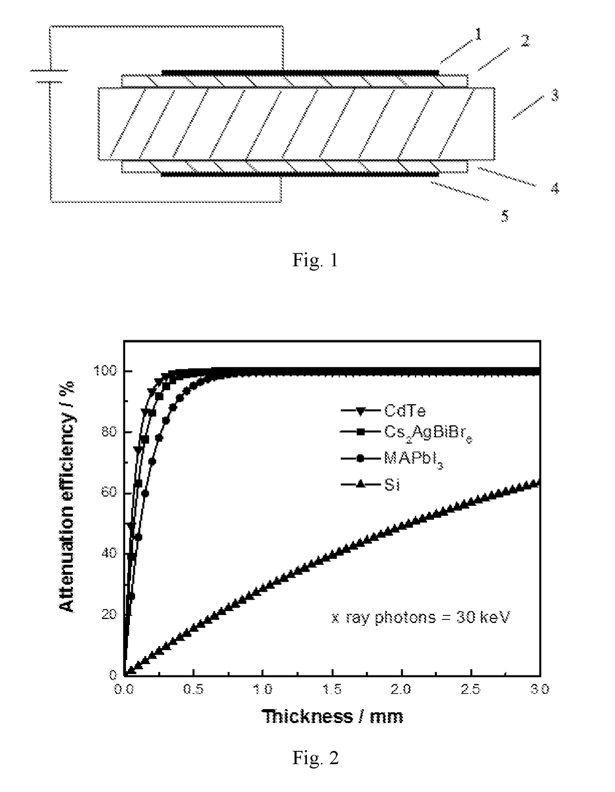
[0035]Gold electrodes with a thickness of 80 nm are then formed on upper and lower surfaces of the crystal by thermal evaporation.

embodiment 2

[0036]In this embodiment, the preparation of cesium silver bismuth bromine (Cs2AgBiBr6) crystal and the manufacturing of a semiconductor radiation detector by adding charge selective contact layers on the crystal will be described.

[0037]Silver bromide (AgBr, 0.188 g, 1 mmol), bismuth bromide (BiBr3, 0.449 g, 1 mmol) and cesium bromide (CsBr, 0.426 g, 2 mmol) are added into a 10 ml solution of hydrobromic acid (HBr), the solution is heated to 130 degrees Celsius to fully dissolve the solute, and then the solution is cooled to 60 degrees Celsius at a rate of 1 degrees Celsius per hour to precipitate the crystal, thereby obtaining the Cs2AgBiBr6 crystal.

[0038]Buckminsterfullerene (C60) is formed on the upper surface of the crystal by thermal evaporation.

[0039]Gold electrodes with a thickness of 80 nm are then formed on the upper and lower surfaces of the crystal by thermal evaporation.

embodiment 3

[0040]In this embodiment, the preparation of cesium silver bismuth bromine (Cs2AgBiBr6) crystal and the manufacturing of a semiconductor radiation detector using this crystal will be described.

[0041]Silver bromide (AgCl, 0.144 g, 1 mmol), bismuth bromide (BiBr3, 0.317 g, 1 mmol) and cesium bromide (CsCl, 0.328 g, 2 mmol) are added into a 10 ml solution of hydrochloric acid (HCl), the solution is heated to 120 degrees Celsius to fully dissolve the solute, and then the solution is cooled to 60 degrees Celsius at a rate of 0.5 degrees Celsius per hour to precipitate the crystal, thereby obtaining the Cs2AgBiCl6 crystal.

[0042]Gold electrodes with a thickness of 80 nm are then formed on upper and lower surfaces of the crystal by thermal evaporation.

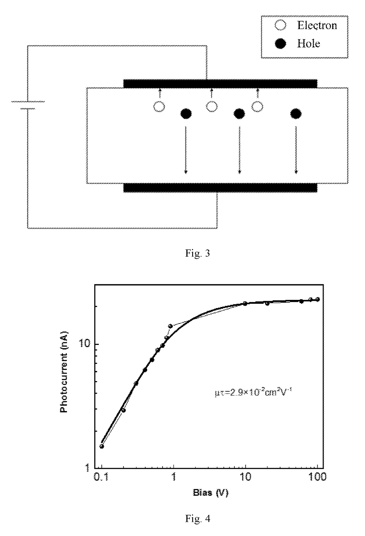
[0043]It can be seen from the embodiments that the semiconductor radiation detector manufactured by the present invention has advantages such as high sensitivity, good stability and environmental friendliness.


PUM


Abstract

The present invention discloses a semiconductor radiation detector based on Bi-based quaternary halide single crystal and a manufacturing method, and relates to the technical field of ray imaging detector manufactured by a semiconductor material. The semiconductor radiation detector in this example includes: a light absorption layer made of Bi-based quaternary halide single crystal; an electron selective contact layer and a hole selective contact layer respectively provided on upper and lower sides of the light absorption layer; and two electrodes which are respectively in contact with the two charge selective contact layers and used as positive and negative electrodes of the device. The semiconductor radiation detector in the present invention has advantages such as high sensitivity, good stability and environmental friendliness.

Description

BACKGROUND OF THE PRESENT INVENTIONField of the Present Invention[0001]The present invention belongs to the technical field of ray imaging detector manufactured by a semiconductor material, and more particularly, relates to a X-ray and gamma-ray imaging detector manufactured by Bi-based quaternary halide single crystal and a manufacturing method thereof.Description of the Related Art[0002]Ray imaging technology uses radioactive rays (such as X-ray and gamma ray) as a medium to obtain information on the structure or function of the detected object to be displayed in the form of an image, provides various industries with technical means for diagnosis, detection and monitoring of the observed objects, and is widely used in medical and health, public safety and high-end manufacturing and other industries. The detector is an important part of the ray imaging equipment. Detectors for detecting radioactive rays generally include gas detector, scintillation detector, and semiconductor detec...

Claims


Application Information

Patent Timeline
Patent Type & Authority Applications(United States)
IPC IPC(8): H01L31/032H01L31/115H01L31/18H01L31/0224
CPCH01L31/032H01L31/022408H01L31/18H01L31/115H01L31/10
Inventor TANG, JIANGPAN, WEICHENGWU, HAODILUO, JIAJUNNIU, GUANGDAZHOU, YING
Owner HUAZHONG UNIV OF SCI & TECH
Why Eureka
Try Eureka