Specially doped perovskite solar cell and preparation method thereof

A solar cell and perovskite technology, applied in circuits, photovoltaic power generation, electrical components, etc., can solve the problems of poor stability of perovskite solar cells, low photoelectric conversion efficiency, poor ability to block water and oxygen, etc., to reduce excitation Sub-recombination probability, improved photoelectric conversion efficiency, and good water and oxygen barrier effect

Active Publication Date: 2020-05-19
UNIV OF ELECTRONICS SCI & TECH OF CHINA
View PDF14 Cites 10 Cited by
  • Summary
  • Abstract
  • Description
  • Claims
  • Application Information

AI Technical Summary

Problems solved by technology

[0004] The purpose of the present invention is to improve and innovate on the shortcomings and problems existing in the background technology, to provide a special doped perovskite solar cell and its preparation method, which is used to solve the problem of low photoelectric conversion efficiency of traditional perovskite solar cells problems, as well as the poor ability to block water and oxygen, and the poor stability of perovskite solar cells

Method used


Image

  • Specially doped perovskite solar cell and preparation method thereof
  • Specially doped perovskite solar cell and preparation method thereof
  • Specially doped perovskite solar cell and preparation method thereof

Examples


specific Embodiment

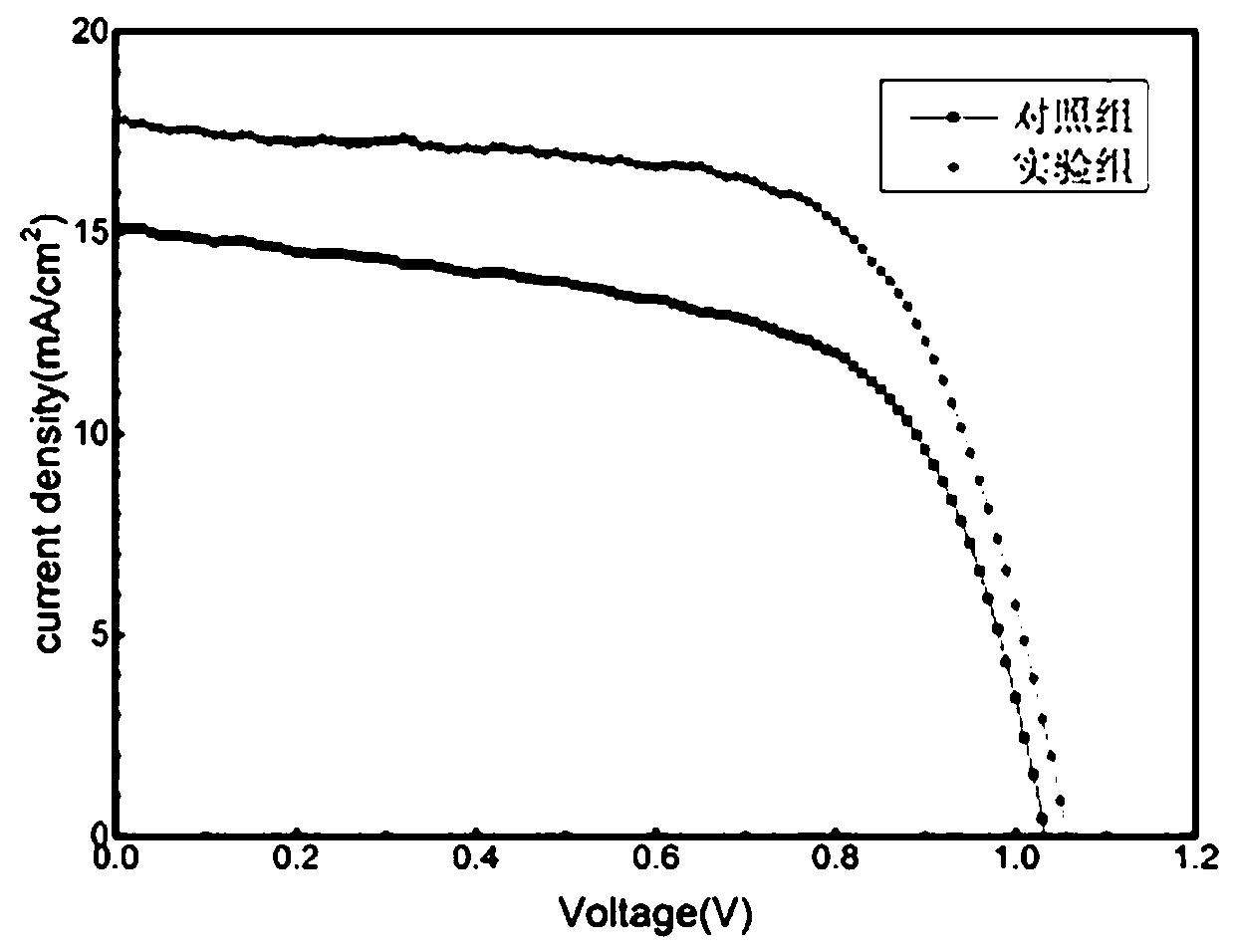
[0037] control group

[0038]The surface of transparent conductive anode ITO is spin-coated with TAPC (spin-coating speed of 3000rpm, spin-coating time of 40s, thickness of 15nm) to prepare a hole transport layer, and the formed film is thermally annealed (annealing temperature 120°C, annealing time 15min); Spin coating of MAPbI on the hole transport layer 3 Precursor solution (mixed with DMF as solvent to form a mixed solution with a solute concentration of 500mg / mL, spin-coating speed is 4000rpm, spin-coating time is 25s, thickness is 500nm) to prepare the perovskite layer, first let the chip rotate at a speed of 4000rpm , then drop the perovskite precursor solution, and then quickly drop the chlorobenzene solution to the perovskite activated carbon layer to inhibit the disordered crystallization of perovskite, and then anneal at 120°C for 20min; The surface is spin-coated with PCBM solution (mixed with chlorobenzene as a solvent to form a mixed solution with a solute conce...

Embodiment 1

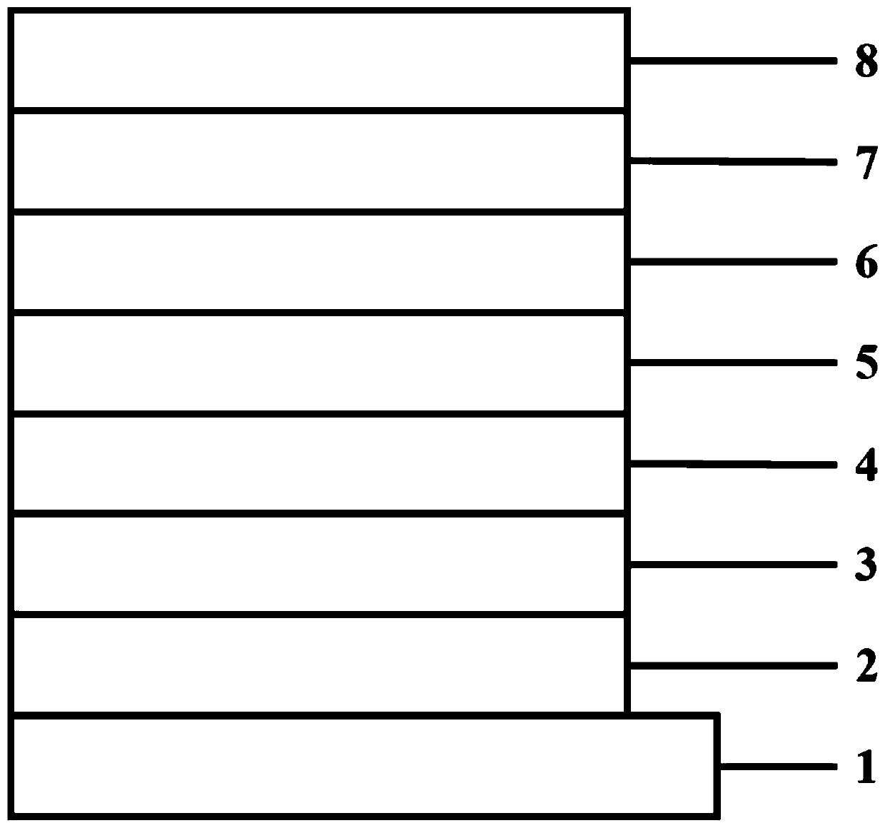
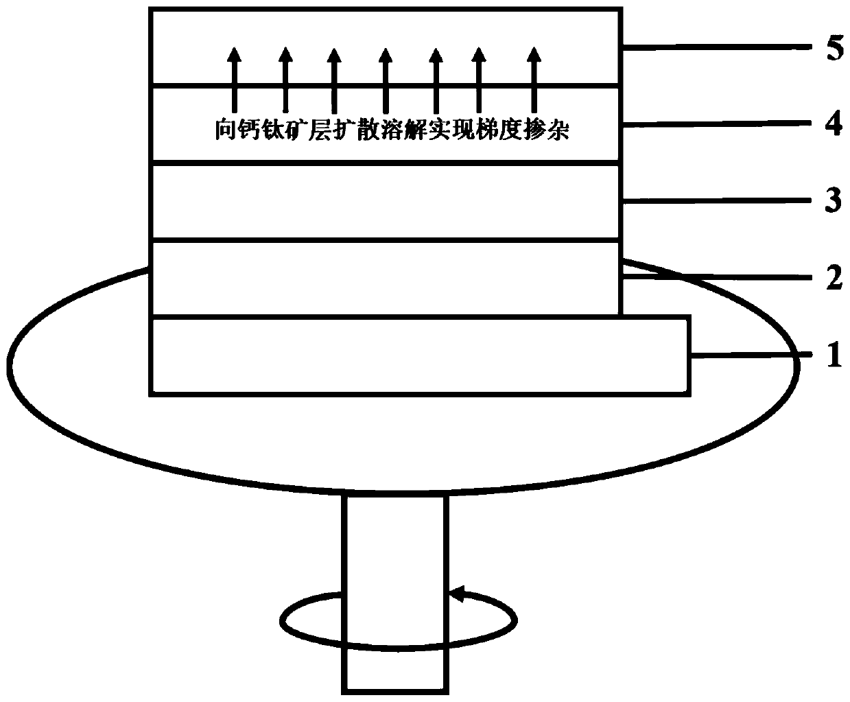
[0041] The substrate composed of the substrate and the transparent conductive anode 2ITO was cleaned, and then dried with nitrogen gas; the surface of the transparent conductive anode 2ITO was spin-coated with TAPC (the spin-coating speed was 3000rpm, the spin-coating time was 40s, and the thickness was 15nm). Hole transport layer 3, and the formed film is subjected to thermal annealing (annealing temperature 120 ℃, annealing time 15min); On the hole transport layer 3, spin-coat passivation doped layer 4 material PEABr, (its solution concentration is 3mg / ml, spin-coating speed is 5000rpm, spin-coating time 30s) passivation doping layer 4, need not annealing; Spin-coat MAPbI on hole transport layer 3 3 Precursor solution (mixed with DMF as solvent to form a mixed solution with a solute concentration of 500mg / mL, spin-coating speed is 4000rpm, spin-coating time is 25s, thickness is 500nm) to prepare the perovskite layer, first let the chip rotate at a speed of 4000rpm , then dr...

Embodiment 2

[0043] The substrate composed of the substrate and the transparent conductive anode 2ITO was cleaned, and then dried with nitrogen gas; the surface of the transparent conductive anode 2ITO was spin-coated with TAPC (the spin-coating speed was 3000rpm, the spin-coating time was 40s, and the thickness was 15nm). Hole transport layer 3, and the formed film is subjected to thermal annealing (annealing temperature 120 ℃, annealing time 15min); On hole transport layer 3, spin-coat passivation doped layer 4 material PEABr, (its solution concentration is 5mg / ml, spin-coating speed is 5000rpm, spin-coating time 30s) passivation doping layer 4, need not annealing; Spin-coat MAPbI on hole transport layer 3 3 Precursor solution (mixed with DMF as solvent to form a mixed solution with a solute concentration of 500mg / mL, spin-coating speed is 4000rpm, spin-coating time is 25s, thickness is 500nm) to prepare the perovskite layer, first let the chip rotate at a speed of 4000rpm , then drop t...


PUM

PropertyMeasurementUnit
thicknessaaaaaaaaaa
thicknessaaaaaaaaaa
thicknessaaaaaaaaaa

Abstract

The invention relates to a specially doped perovskite solar cell and a preparation method thereof. The perovskite solar cell is sequentially provided with a transparent substrate, a conductive anode,a hole transport layer, a passivation doping layer, a perovskite active layer, an electron transport layer, a hole blocking layer and a metal cathode from bottom to top, the passivation doping layer is made of a two-dimensional perovskite precursor material or organic ammonium salt, and the thickness of the passivation doping layer is 0.1-10 nm. Compared with a traditional perovskite solar cell, the photoelectric conversion efficiency is higher, the water and oxygen blocking capacity is better, and the stability of the perovskite solar cell is better.

Description

technical field [0001] The invention relates to the technical field of organic photoelectric devices in electronic components, in particular to a special doped perovskite solar cell and a preparation method thereof. Background technique [0002] The development of human civilization depends on the most basic material basis - energy. In modern society, we cannot do without the use of energy in every aspect of our daily work, life, and production. With the rapid development of the global economy, we are in a state of embarrassment in the use of energy. Fossil energy sources currently being developed and utilized on a large scale include oil, coal, natural gas and other energy sources. The reserves of these energy sources are finite and are likely to be permanently depleted in the near future. In addition, the exploitation and use of fossil energy will cause environmental pollution. In order to fundamentally solve the energy problem and the environmental problems caused by ...

Claims


Application Information

Patent Timeline
Patent Type & Authority Applications(China)
IPC IPC(8): H01L51/42H01L51/46H01L51/48
CPCH10K71/12H10K85/30H10K30/00Y02E10/549
Inventor 李嘉文郑丁杨根杰于军胜
Owner UNIV OF ELECTRONICS SCI & TECH OF CHINA
Why Eureka
Try Eureka