Non-doped crystalline silicon heterojunction perovskite laminated solar cell structure and preparation method thereof

A technology of stacked sun and perovskite, applied in the field of solar cells, can solve the problems of poor stability of perovskite and low efficiency of crystalline silicon, and achieve the effect of improving open circuit voltage and photoelectric conversion efficiency

Inactive Publication Date: 2020-06-05
DALIAN INST OF CHEM PHYSICS CHINESE ACAD OF SCI
View PDF4 Cites 8 Cited by
  • Summary
  • Abstract
  • Description
  • Claims
  • Application Information

AI Technical Summary

Problems solved by technology

This cell combines the advantages of non-doped crystalline silicon heterojunction cell and perovskite solar cell technology, and the synergistic effect produced is far greater than that of a single technol

Method used


Image

  • Non-doped crystalline silicon heterojunction perovskite laminated solar cell structure and preparation method thereof

Examples


Embodiment 1

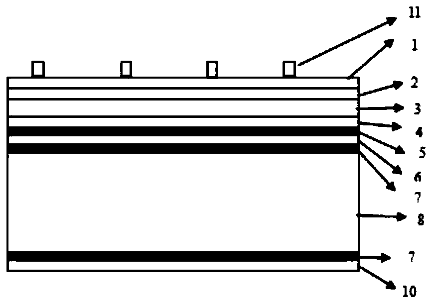
[0045] The non-doped crystalline silicon heterojunction perovskite tandem solar cell of this embodiment is manufactured through the following steps:

[0046] (1) Etch a 180 μm n-type silicon wafer with an n-type crystal orientation in a KOH solution of 80-90 degrees to obtain a pyramid structure, and then use the RCA method to clean it.

[0047] (2) Wet oxidation is adopted, and the cleaned silicon wafer is soaked in concentrated nitric acid at 120 degrees for oxidation to form a silicon dioxide layer for passivation. Minority lifetime 3ms.

[0048] (3) A MgF electron transport layer is deposited on the back of the passivated crystalline silicon by thermal evaporation technology. Thickness is 10nm

[0049] (4) Deposit MoO on the front side of the passivated crystalline silicon by thermal evaporation or magnetron sputtering x Hole transport transport layer. Thickness is 10nm

[0050] (5) Deposit a transparent conductive film ITO on the electron transport layer by thermal ...

Embodiment 2

[0058] (1) Etch a 180 μm n-type silicon wafer with an n-type crystal orientation in a KOH solution of 80-90 degrees to obtain a pyramid structure, and then use the RCA method to clean it.

[0059] (2) Wet oxidation is adopted, and the cleaned silicon wafer is soaked in concentrated nitric acid at 120 degrees for oxidation to form a silicon dioxide layer for passivation. Minority lifetime 3ms.

[0060] (3) Deposit TiO on the back of passivated crystalline silicon by thermal evaporation technology x electron transport layer. Thickness is 10nm

[0061] (4) On the front side of the passivated crystalline silicon, NiO is deposited by thermal evaporation or magnetron sputtering technology x Hole transport transport layer. Thickness is 10nm

[0062] (5) Deposit a transparent conductive film ITO on the electron transport layer by thermal evaporation. On the transparent conductive film ITO, the silver back electrode was deposited by thermal evaporation technology.

[0063] (6) ...


PUM

PropertyMeasurementUnit
Thicknessaaaaaaaaaa
Thicknessaaaaaaaaaa
Thicknessaaaaaaaaaa

Abstract

The invention belongs to the technical field of solar cells, and particularly relates to a crystalline silicon substrate perovskite laminated heterojunction cell structure and a preparation method. The laminated heterojunction cell sequentially comprises a transparent conductive film (TCO), an electron transport layer, a perovskite layer, a hole transport layer, an interface layer, an electron transport layer, a passivation layer, N-type monocrystalline silicon, a passivation layer, a hole transport layer, a transparent conductive film and a back electrode from the front surface to the back surface. The cell prepared by the invention combines the advantages of a non-doped crystalline silicon heterojunction cell and a perovskite solar cell technology, the generated synergistic effect is fargreater than that of a single technology, and a plurality of problems, such as low crystalline silicon efficiency and poor perovskite stability, generated when the two technologies in the backgroundtechnology are independently adopted are well solved.

Description

technical field [0001] The invention belongs to the technical field of solar cells, and in particular relates to a non-doped n-type crystalline silicon perovskite heterojunction cell structure and a preparation method thereof. Background technique [0002] Non-doped crystalline silicon heterojunction cells have attracted much attention in recent years due to their simple structure, low manufacturing cost, high open circuit voltage and high conversion efficiency. However, the properties of the transport layer limit the improvement of the open circuit voltage and efficiency of the battery to a certain extent. Using a battery with a large band gap as a fixed battery and a non-doped crystalline silicon heterojunction battery to form a stacked structure can improve the open circuit voltage, spectral response and theoretical conversion efficiency limit of the battery. In recent years, perovskite batteries have developed rapidly, and their conversion efficiency has risen from less...

Claims


Application Information

Patent Timeline
IPC IPC(8): H01L51/42H01L51/48
CPCH10K71/10H10K30/10Y02E10/549Y02P70/50
Inventor 刘生忠焦玉骁王辉曹越先杜敏永段连杰孙友名王开秦炜
Owner DALIAN INST OF CHEM PHYSICS CHINESE ACAD OF SCI
Why Eureka
Try Eureka