LED epitaxial growth method

An epitaxial growth and alternate growth technology, which is applied in the direction of electrical components, circuits, semiconductor devices, etc., can solve the problems of lattice mismatch, weakened antistatic ability of LED devices, and ineffective reduction of dislocation density.

Active Publication Date: 2020-06-09
XIANGNENG HUALEI OPTOELECTRONICS
View PDF5 Cites 2 Cited by
  • Summary
  • Abstract
  • Description
  • Claims
  • Application Information

AI Technical Summary

Problems solved by technology

[0002] At present, the LED epitaxial structure grown by metal chemical vapor deposition method MOCVD is prone to defects of lattice mismatch between the substrate and the gallium nitride layer. The defects include point dislocations, ductile dislocations and screw dislocations. The error density is between 1×10 10 ~3×10 10 piece/m 2 , the existence of dislocations destroys the original crystal ordering of gallium nitride, and brings many negative effects on LED devices. For example, screw dislocations make the LED epitaxial structure extend from the bottom layer of the epitaxial layer to the surface of the epitaxial layer, passing through the light-emitting layer, and providing LED devices The leakage current of the LED device provides a path, and the leakage cu

Method used


Image

  • LED epitaxial growth method
  • LED epitaxial growth method

Examples


Embodiment 1

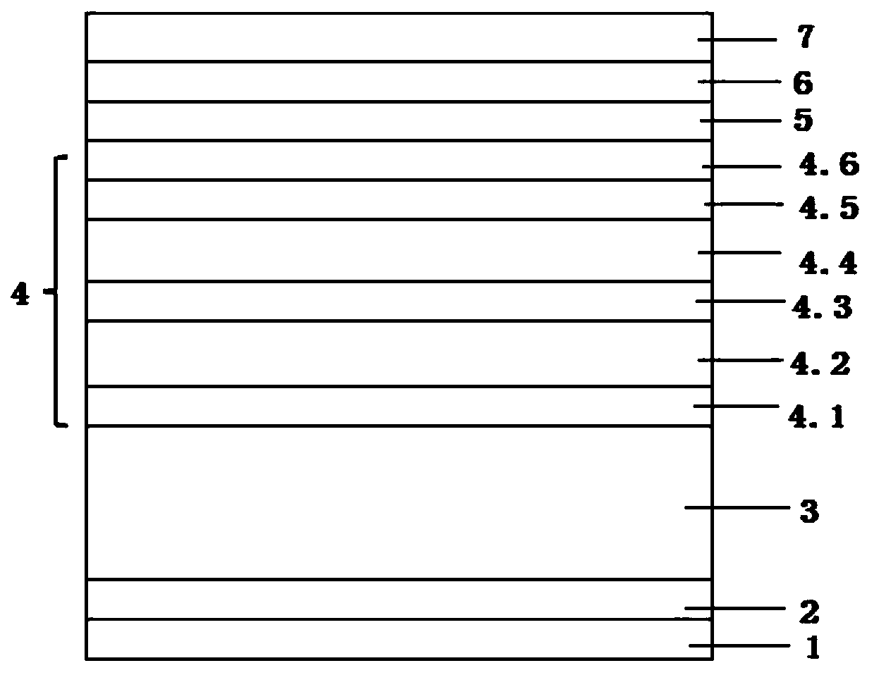
[0045] A LED epitaxial growth method, including the process of growing a composite N-type layer, the epitaxial growth method is specifically as follows:

[0046] Step 1, processing the substrate 1;

[0047] Step 2, growing a low-temperature buffer gallium nitride layer 2 on the substrate 1;

[0048] Step 3, growing an undoped gallium nitride layer 3;

[0049] Step 4, growing a composite N-type layer 4;

[0050] Step 5, growing the multi-quantum well light-emitting layer 5;

[0051] Step 6, growing an electron blocking layer 6 doped with aluminum and magnesium;

[0052] Step 7, growing a high-temperature P-type gallium nitride layer 7 doped with magnesium;

[0053] Step 8. Under the condition of temperature of 750-800° C. and pressure of 500-800 mbar, anneal in the furnace for 25-30 minutes, turn off the heating system and gas supply system, and then cool down with the furnace.

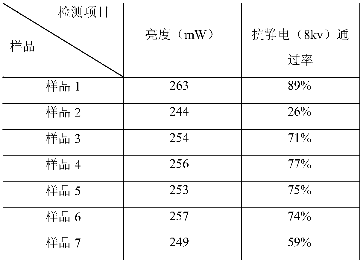
[0054] In Example 1, a high-brightness gallium nitride-based LED epitaxial wafer was grown on ...


PUM

PropertyMeasurementUnit
Thicknessaaaaaaaaaa
Thicknessaaaaaaaaaa
Thicknessaaaaaaaaaa

Abstract

The invention provides an LED epitaxial growth method for improving antistatic capability and luminous efficiency. The LED epitaxial growth method specifically comprises the steps of 1, processing a substrate; 2, growing a low-temperature buffer layer gallium nitride layer on the substrate; 3, growing an undoped gallium nitride layer; 4, growing a composite N-type layer; 5, growing a multi-quantumwell light-emitting layer; 6, growing an electron barrier layer doped with aluminum and magnesium; 7, growing a magnesium-doped high-temperature P-type gallium nitride layer; and 8, annealing in a furnace for 25-30 minutes under the conditions that the temperature is 750-800 DEG C and the pressure is 500-800mbar, closing a heating system and a gas supply system, and cooling along with the furnace. According to the epitaxial growth method, the bottom stress is greatly released, the bottom dislocation density is reduced, the gallium nitride crystal quality is improved, the current expansion isimproved, the antistatic performance of the LED is improved, and the light output power of the LED is also improved.

Description

technical field [0001] The invention relates to the technical field of LEDs, in particular to an LED epitaxial growth method. Background technique [0002] At present, the LED epitaxial structure grown by metal chemical vapor deposition method MOCVD is prone to defects of lattice mismatch between the substrate and the gallium nitride layer. The defects include point dislocations, ductile dislocations and screw dislocations. The error density is between 1×10 10 ~3×10 10 piece / m 2 , the existence of dislocations destroys the original crystal ordering of gallium nitride, and brings many negative effects on LED devices. For example, screw dislocations make the LED epitaxial structure extend from the bottom layer of the epitaxial layer to the surface of the epitaxial layer, passing through the light-emitting layer, and providing LED devices The leakage current of the LED device provides a path, and the leakage current of the LED device accelerates the aging of the device, and ...

Claims


Application Information

Patent Timeline
IPC IPC(8): H01L33/00H01L33/32H01L33/14H01L33/12H01L21/02
CPCH01L21/02458H01L21/0254H01L21/0262H01L33/0075H01L33/12H01L33/145H01L33/325
Inventor 林传强
Owner XIANGNENG HUALEI OPTOELECTRONICS
Why Eureka
Try Eureka