Check patentability & draft patents in minutes with Patsnap Eureka AI!

Preparation method and system of polycrystalline silicon film

A polysilicon thin film and wafer technology, applied in semiconductor/solid-state device manufacturing, electrical components, circuits, etc., can solve problems such as insufficiency and difficulty in improving the yield of MEMS products, improve efficiency, save process and testing steps, cost reduction effect

Inactive Publication Date: 2020-06-12
SEMICON MFG ELECTRONICS (SHAOXING) CORP
View PDF0 Cites 2 Cited by
  • Summary
  • Abstract
  • Description
  • Claims
  • Application Information

AI Technical Summary

Problems solved by technology

However, in process design, when the resistance (RS) of the polysilicon thin film of MEMS products is required to be between 850Ω~950Ω, and the stress is between 60Mpa~75Mpa, if the existing furnace tube technology adjustment and conventional process parameters (temperature / pressure / gas flow rate / time, etc.) monitoring, the resistance and stress of the finally formed polysilicon thin film deviate from the corresponding target value by 5% to 10%, which makes it difficult to improve the yield rate of MEMS products, or even fail to meet the requirements.

Method used


Image

  • Preparation method and system of polycrystalline silicon film
  • Preparation method and system of polycrystalline silicon film
  • Preparation method and system of polycrystalline silicon film

Examples


Embodiment Construction

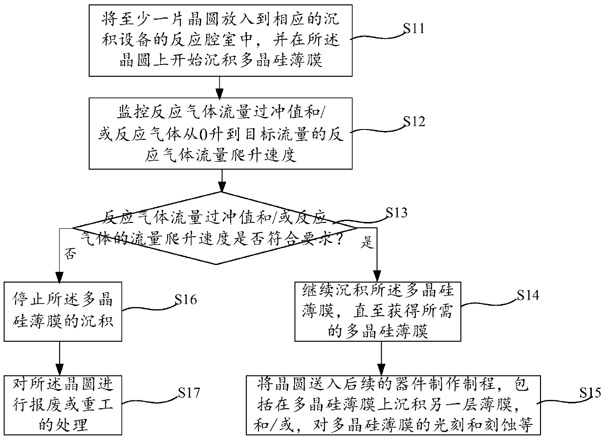
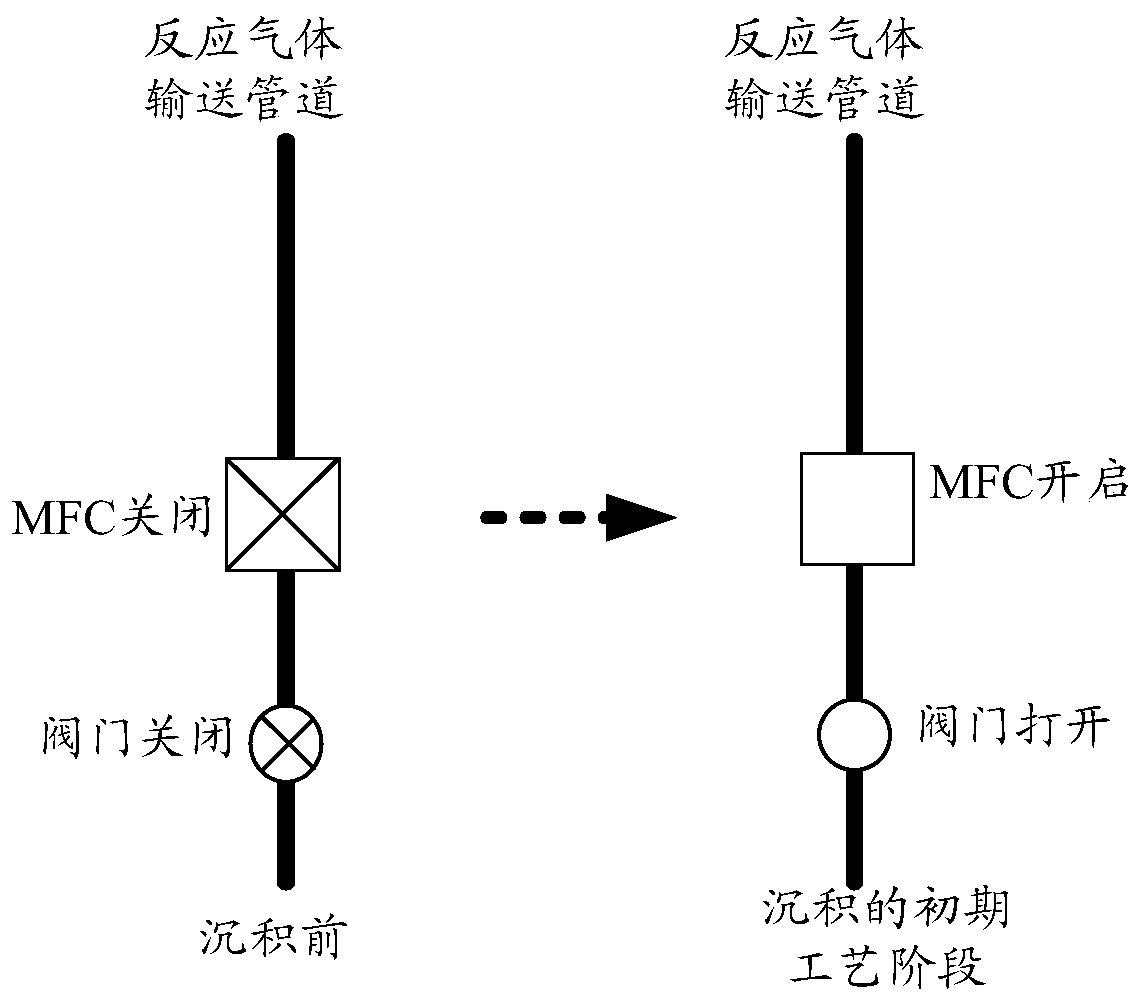
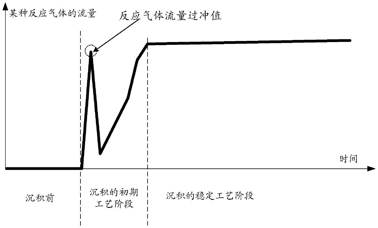
[0027] The technical solutions proposed by the present invention will be described in further detail below in conjunction with the accompanying drawings and specific embodiments. The advantages and features of the present invention will become clearer from the following description. It should be noted that all the drawings are in a very simplified form and use imprecise scales, and are only used to facilitate and clearly assist the purpose of illustrating the embodiments of the present invention. In addition, the meaning of "and / or" in this application document is to choose one or both; The mass flow meter (MFC) and other valves open the flow overshoot value (over shoot); The time required for the flow to go from 0 to the flow value set in the recipe.

[0028] The inventors have found that the overshoot value (MFC peak) of the reactant gas flow rate and the ramp rate (MFC ramp) of the reactant gas in the initial process stage of depositing polysilicon film both have a great ...


PUM

PropertyMeasurementUnit
electrical resistanceaaaaaaaaaa
thicknessaaaaaaaaaa

Abstract

The invention provides a preparation method and system of a polycrystalline silicon thin film. When a polycrystalline silicon thin film is deposited, a reaction gas flow overshoot value and / or a reaction gas flow climbing speed (i.e., the time required for raising the flow of the reaction gas from 0 to the target flow) is monitored; and when it is found that the monitored reaction gas flow overshoot value and / or reaction gas flow climbing speed do / does not meet the requirement (i.e., abnormity occurs), the deposition process of the polycrystalline silicon thin film can be stopped in time. Therefore, according to the technical scheme, the defective wafer can be found earlier, deposition of the polycrystalline silicon thin film is directly stopped, the defective wafer is scrapped, subsequentprocesses and testing steps are omitted, efficiency is improved, and cost is reduced.

Description

technical field [0001] The invention relates to the technical field of integrated circuit manufacturing, in particular to a method and system for preparing a polysilicon thin film. Background technique [0002] As an important semiconductor thin film material, polysilicon thin film has already attracted people's attention, and it has been widely used in the manufacture of integrated circuits and various electronic devices. , is an ideal structural layer material, so polysilicon thin film is widely used as the basic structural material in microelectromechanical systems (MEMS). [0003] For example, existing MEMS microphone products generally use a doped polysilicon film as a diaphragm. The main process indicators of the doped polysilicon film include thickness, grain, resistance (RS) and stress (Stress), and conventional processes rarely monitor resistance. and stress, but these two data are very important in MEMS products such as microphones, which will have a great impact ...

Claims


Application Information

Patent Timeline
Patent Type & Authority Applications(China)
IPC IPC(8): H01L21/02H01L21/67
CPCH01L21/02123H01L21/0226H01L21/02271H01L21/67011H01L21/67253
Inventor 刘鹏蔡丹华李勇
Owner SEMICON MFG ELECTRONICS (SHAOXING) CORP
Features
  • R&D
  • Intellectual Property
  • Life Sciences
  • Materials
  • Tech Scout
  • Unparalleled Data Quality
  • Higher Quality Content
  • 60% Fewer Hallucinations
Learn More