

Graphene semiconductor preparation device and method
A technology for graphene semiconductors and preparation devices, applied in graphene, chemical instruments and methods, inorganic chemistry, etc., can solve the problems affecting the promotion and application of graphene devices, the large impact of graphene morphology and performance, and the difficulty of transferring graphene, etc. problems, to achieve the effect of improving photoelectric conversion efficiency, wide applicability, and good uniformity
- Summary
- Abstract
- Description
- Claims
- Application Information
AI Technical Summary
Problems solved by technology
Method used
Image

Examples
preparation example Construction
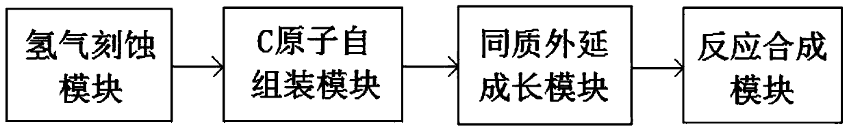
[0024] A kind of graphene semiconductor preparation method, comprises the following steps:
[0025] I. Provide a SiC substrate, use the etching effect of hydrogen on the substrate at 1450-1600°C to planarize the surface of the SiC substrate, etch for 25-35min to form a stepped array shape with atomic-level flatness Surface appearance; SiC substrate is one of 4H-SiC, 6H-SiC, 3C-SiC single crystals. SiC substrate material can provide the C source required for graphene preparation. Since the SiC crystal is selected, it is determined that the graphene must be processed under high temperature conditions.
[0026] Etching using hydrogen gas can remove mechanical damage and scratches caused by the grinding and polishing process of the SiC surface, so that the SiC surface presents a regular step shape. The reaction of H2 and SiC at high temperature will generate gaseous hydrocarbons such as C2H2, etc., and also generate some basic Si-based by-products and other impurities. However,...
Embodiment 1
[0042] A kind of graphene semiconductor preparation method, comprises the following steps:
[0043] 1. Provide a SiC substrate, use the etching effect of hydrogen on the substrate at 1450 ° C to planarize the surface of the SiC substrate, etch for 25 minutes, so as to form a surface with a stepped array morphology with atomic-level flatness; SiC substrate is 4H-SiC single crystal
[0044] II. The temperature of the SiC substrate is raised to 1000°C in an argon atmosphere of 1.5L / min, so that the self-assembly process of C atoms can be carried out more fully, and a large-area and uniform graphene film can be produced; the pressure of argon is controlled in 2×10 3 Below Pa.
[0045] III. In an ultra-high vacuum environment, continue to heat the surface of the SiC substrate to 1400°C to break the carbon-silicon bond on the surface of the SiC substrate, and the Si atoms will desorb from the surface before the sublimation of the C atoms, and the surface is rich in The set of C ato...
Embodiment 2
[0050] A kind of graphene semiconductor preparation method, comprises the following steps:
[0051] 1. Provide a SiC substrate, use the etching effect of hydrogen on the substrate at 1500 ° C to planarize the surface of the SiC substrate, etch for 30 minutes, so as to form a surface with a step array morphology with atomic-level flatness; SiC substrate 6H-SiC single crystal;
[0052] II. Raise the temperature of the SiC substrate to 1050°C in an argon atmosphere of 1.5L / min, so that the self-assembly process of C atoms can be carried out more fully, and a large-area and uniform graphene film can be produced; the pressure of argon is controlled in 2×10 3 Below Pa.
[0053] III. In an ultra-high vacuum environment, continue to heat the surface of the SiC substrate to 1450°C to break the carbon-silicon bond on the surface of the SiC substrate, and the Si atoms will desorb from the surface before the sublimation of the C atoms, and the surface is rich in The set of C atoms is r...
PUM
| Property | Measurement | Unit |
|---|---|---|
| particle diameter | aaaaa | aaaaa |
| particle diameter | aaaaa | aaaaa |
| particle diameter | aaaaa | aaaaa |
Abstract
Description
Claims
Application Information