

Vertical structure LED chip with double-sided transparent electrodes and preparation method of vertical structure LED chip
A technology of LED chips and transparent electrodes, which is applied in circuits, electrical components, semiconductor devices, etc., can solve problems such as poor current expansion and unstable voltage, and achieve the effects of poor current expansion, stable product voltage, and reduced heat generation
- Summary
- Abstract
- Description
- Claims
- Application Information
AI Technical Summary
Problems solved by technology
Method used
Image

Examples
preparation example Construction
[0050] A method for preparing a vertical structure LED chip with double-sided transparent electrodes, said method comprising the following steps:
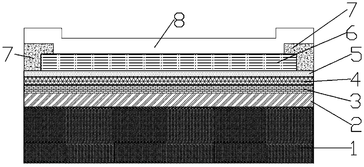
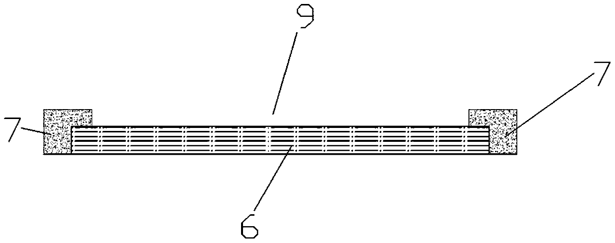
[0051] Step S1, using MOCVD to grow epitaxial layer 6 on silicon, sapphire, SiC and other substrates to form LED epitaxial wafers;
[0052] Step S2, growing a p-plane transparent electrode 5 on the LED epitaxial wafer by using CVD or PVD or vapor deposition or spin coating;
[0053] Step S3, using electron beam evaporation or PVD to cover the entire surface of the p-side transparent electrode 5 and the epitaxial layer 6 with the reflective metal layer 4;
[0054] Step S4, using electron beam evaporation or PVD method to cover the entire surface of the reflective metal layer 4 with the protective metal layer 3 and the bonding metal layer 2;
[0055] Step S5, making a bonding metal layer on the supporting conductive substrate 1 by means of electron beam evaporation or PVD;
[0056] Step S6, bonding the samples obtained in step S4 a...
Embodiment 1
[0064] (1) Using MOCVD epitaxial technology to grow LED epitaxial wafers with 2um-8um epitaxial layers on Si substrates;
[0065] (2) Use acetone and isopropanol for organic cleaning for 5 minutes to remove organic dirt;
[0066] (3) Use SPM solution for pickling to remove inorganic metal dirt and organic dirt;
[0067] (4) Rinse and dry, and use CVD equipment to grow 200nm graphene at 300 degrees;
[0068] (5) Al metal 200nm is deposited on the entire surface by electron beam evaporation.
[0069] (6) Electron beam evaporation TiPtTiPt (Ti20nm-200nm, Pt20nm-300nm) protective layer and NiSn (Ni100nm-800nm, Sn100nm-2000nm) bonding metal layer
[0070] (7) Using an electron beam evaporation process, a NiSn (Ni100nm-800nm, Sn100nm-2000nm) bonded metal layer is evaporated on the Si substrate with high conductivity.
[0071] (8) The finished samples of (10) and (11) are bonded by a bonder, and the silicon substrate is removed by grinding and chemical etching.
[0072] (9) Use h...
PUM
| Property | Measurement | Unit |
|---|---|---|
| Thickness | aaaaa | aaaaa |
| Thickness | aaaaa | aaaaa |
| Thickness | aaaaa | aaaaa |
Abstract
Description
Claims
Application Information