

Microsystem packaging method
A packaging method and microsystem technology, applied in the field of microsystems, can solve problems such as inability to reuse and narrow application range of microsystems, and achieve the effects of expanding applicable scenarios, improving integration and mass production, and improving openness
- Summary
- Abstract
- Description
- Claims
- Application Information
AI Technical Summary
Problems solved by technology
Method used
Image

Examples
preparation example Construction
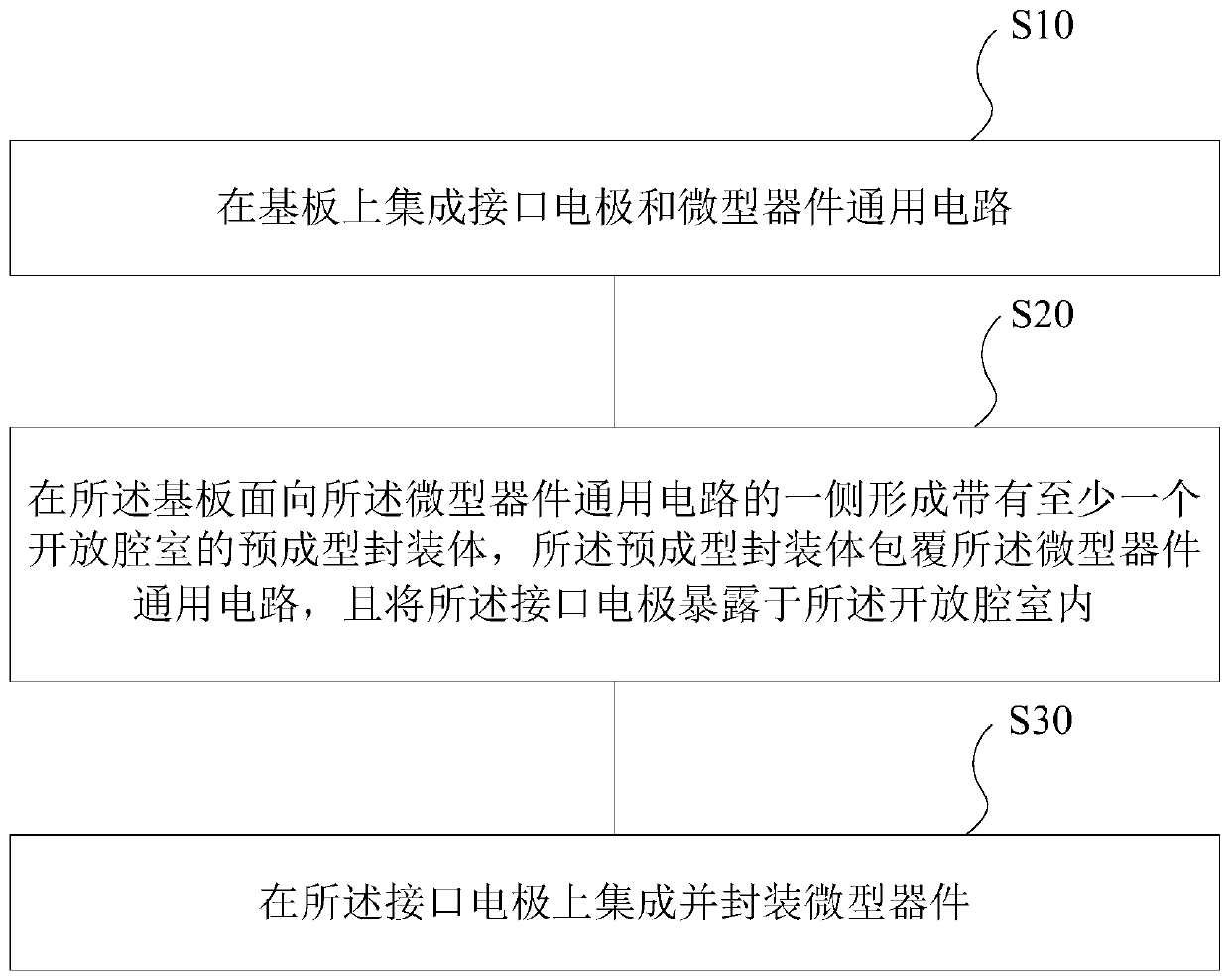
[0043] The preparation of existing sensing microsystems includes three main parts: microsensor integration, microelectronic integration, and packaging and molding. Among them, microelectronics integration and packaging molding have relatively uniform industry standards, while microsensors face natural objects with many types and various parameters, so the standards for various application industries are not uniform. Therefore, considering that the existing sensing microsystems rely on one-time molding process, the process coupling relationship between the integration of microsensors and the integration of other common parts (including microelectronics integration and package molding) is too tight, resulting in premature sealing of microsensors In the microsystem, there is a lack of open microsystem packaging and processing solutions. This application provides a microsystem packaging method, which can keep the microsystem body (microelectronic circuit and package body) unchanged...
Embodiment 1
[0067] Embodiment 1: The structure and process of the precision machining open microsystem and its secondary integration of mechanical microsensors.
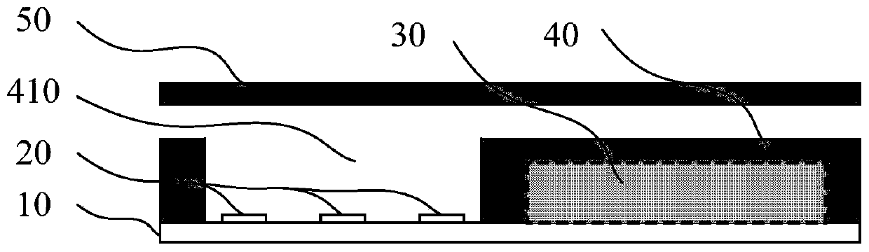
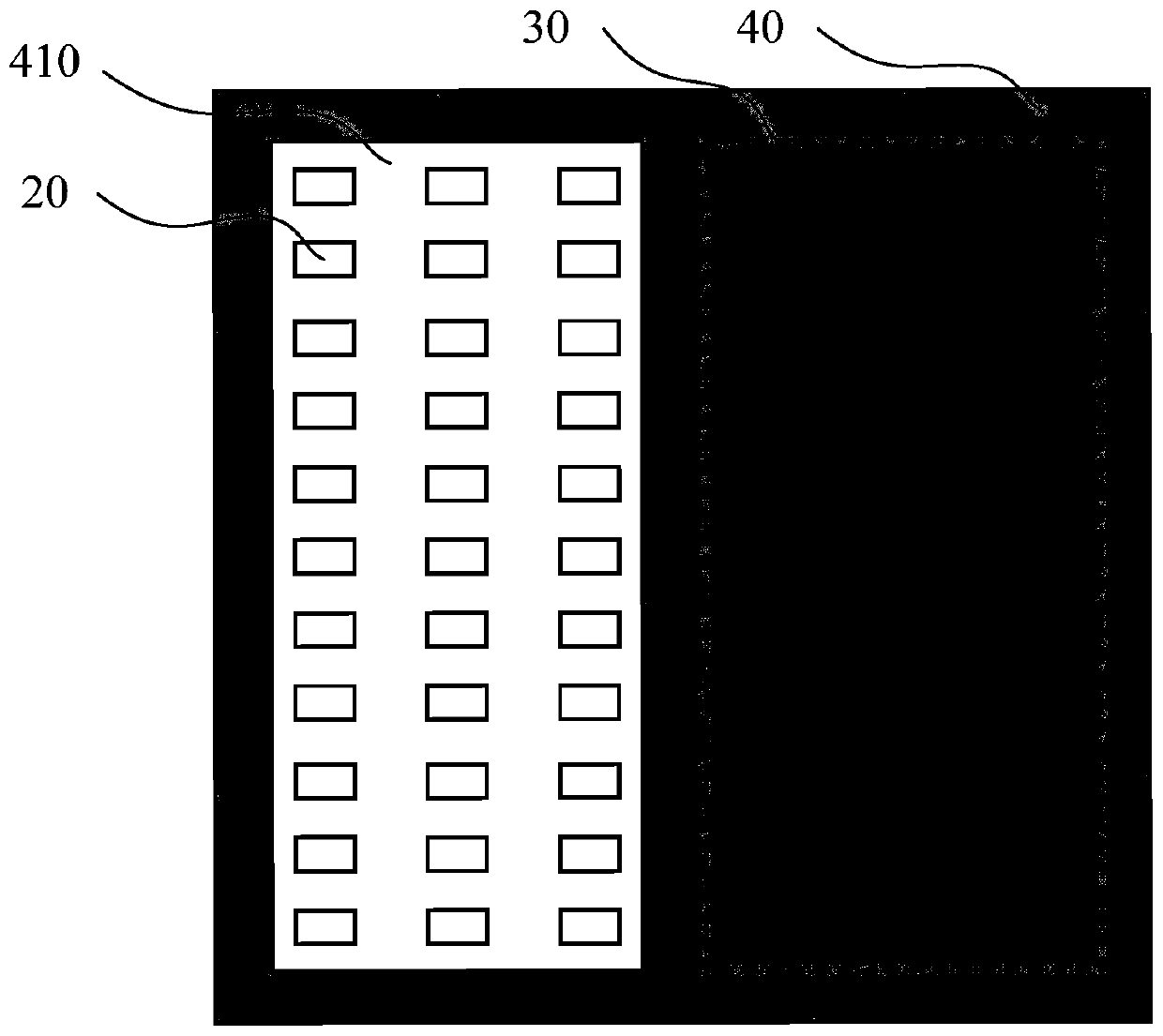
[0068] Please also see Figure 2-Figure 3 , to describe the specific structure of the prefabrication of the open microsystem in this embodiment. Wherein, the substrate 10 can be an FR4 printed circuit board with a size of 10mm×10mm×0.8mm, and the open interface electrodes 20 integrally formed on the upper surface thereof are two sets of electrode arrays, and each group of arrays is distributed on an area of 4mm×4mm. Each includes five 0.8mm×0.5mm immersion gold copper pads on the surface, and the thickness of the immersion gold is 2 microns. The micro-device general circuit 30 can be a general circuit composed of AD8235 differential instrumentation amplifier, CC1350 wireless microcontroller, RT9078 power management chip and several 0201 package resistors, capacitors, and inductors, occupying an area of 8mm×4mm, which is dif...
Embodiment 2
[0077] Embodiment 2: The structure and process of cofferdam filling open microsystem and its secondary integration of magnetic intensity microsensors.
[0078] Please also see Figure 2-Figure 3 , to describe the specific structure of the prefabrication of the open microsystem in this embodiment. Among them, the substrate 10 can be a high-density BT resin substrate of 12mm×12mm×0.5mm, and the open interface electrode 20 can be a group of electrode arrays located on the upper surface of the substrate 10 and integrally formed with the substrate 10, distributed in a 9.8mm×4.9mm In the area of , there are 27 gold-plated copper pads of 0.8mm×0.5mm in total, and the thickness of the gold-plated layer is 2 microns. The micro-device general circuit 30 can be a general circuit located on the upper surface of the substrate 10 and composed of AD8235 differential instrumentation amplifier, CC1350 wireless microcontroller, RT9078 power management chip and several 0201 packaged resistors...
PUM
 Abstract
Description
Claims
Application Information