

Amorphous silicon/crystalline silicon heterojunction solar cell and preparation method thereof
A solar cell and amorphous silicon technology, which is applied in circuits, photovoltaic power generation, electrical components, etc., can solve the problems affecting the service life, economic benefits, and attenuation of amorphous silicon/crystalline silicon heterojunction solar cells, so as to improve the photovoltaic power generation. Conversion efficiency, improved stability, optimized effect of anti-reflection effect
- Summary
- Abstract
- Description
- Claims
- Application Information
AI Technical Summary
Problems solved by technology
Method used
Image

Examples
preparation example Construction
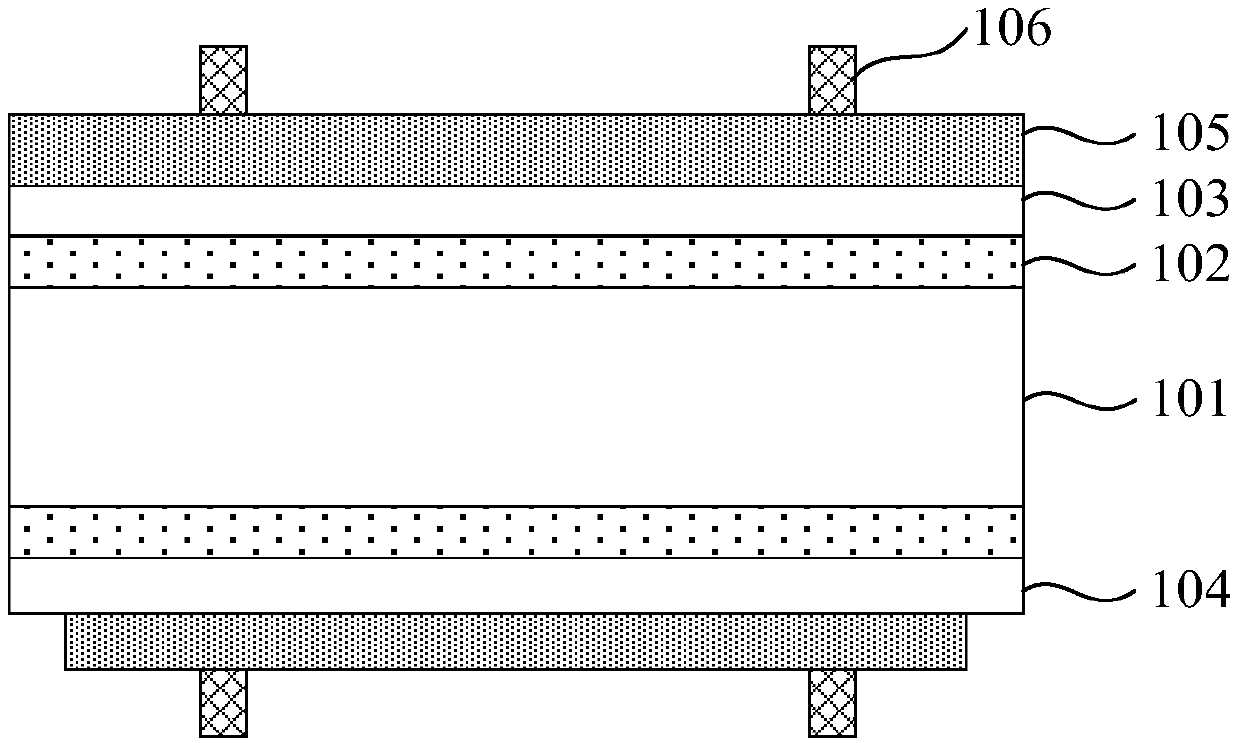
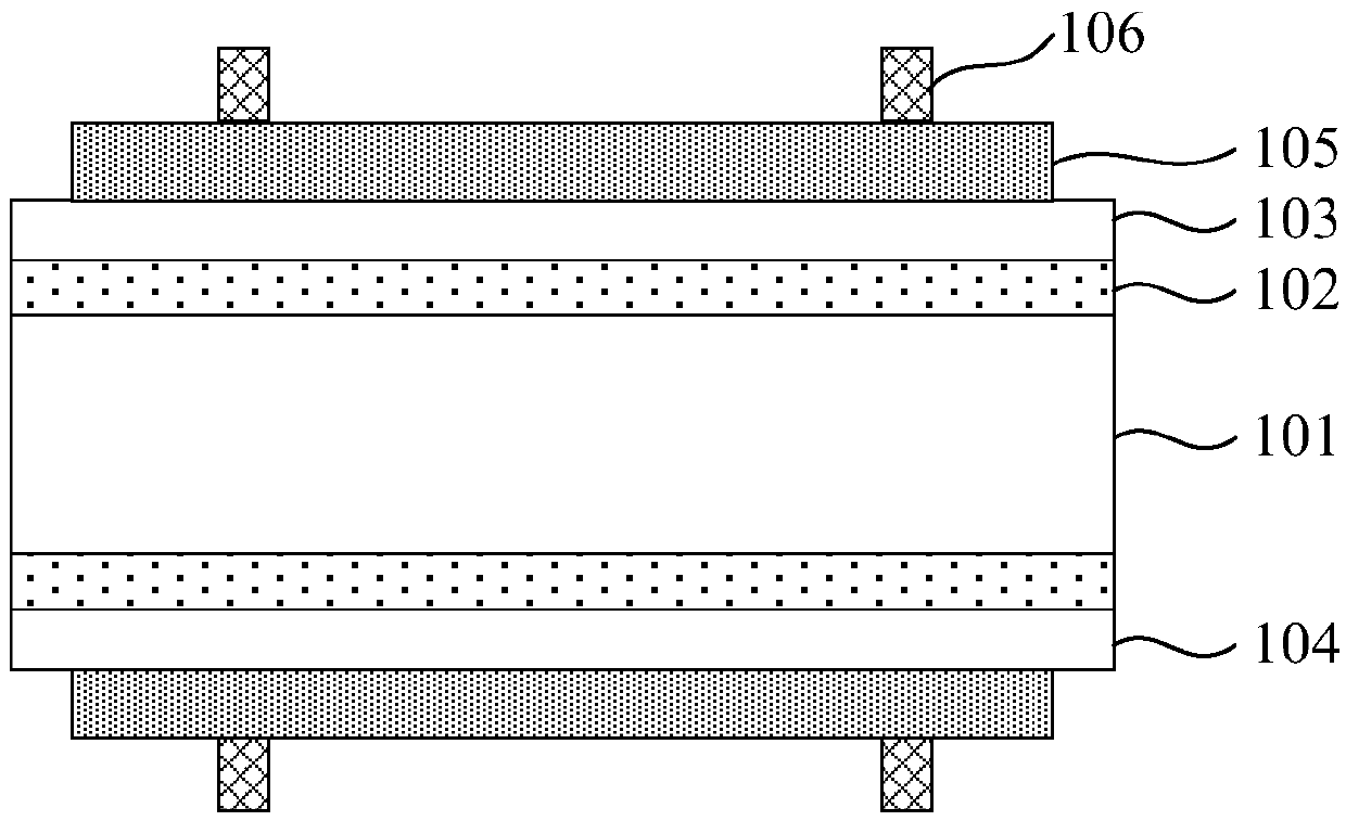
[0059] There are many existing methods for preparing the transparent conductive oxide thin film 105, and preparing the transparent conductive oxide thin film 105 with low temperature and low damage is the key to obtaining the efficient amorphous silicon / crystalline silicon heterojunction solar cell . Currently, magnetron sputtering (Sputtering) coating technology and reactive plasma deposition (RPD) are two optional technologies for commercially preparing the transparent conductive oxide thin film 105 . As mentioned above, since the transparent conductive oxide film 105 acts as both a conductive layer and an anti-reflection layer, it is required in structural design to cover as much as possible the surface of the amorphous silicon, so as to give full play to its conductivity and anti-reflection layer. Dual function of anti-reflection. However, since the N-type single crystal silicon wafer 101 is relatively thin (100 μm to 200 μm), the transparent conductive oxide film 105 is ...
Embodiment 1
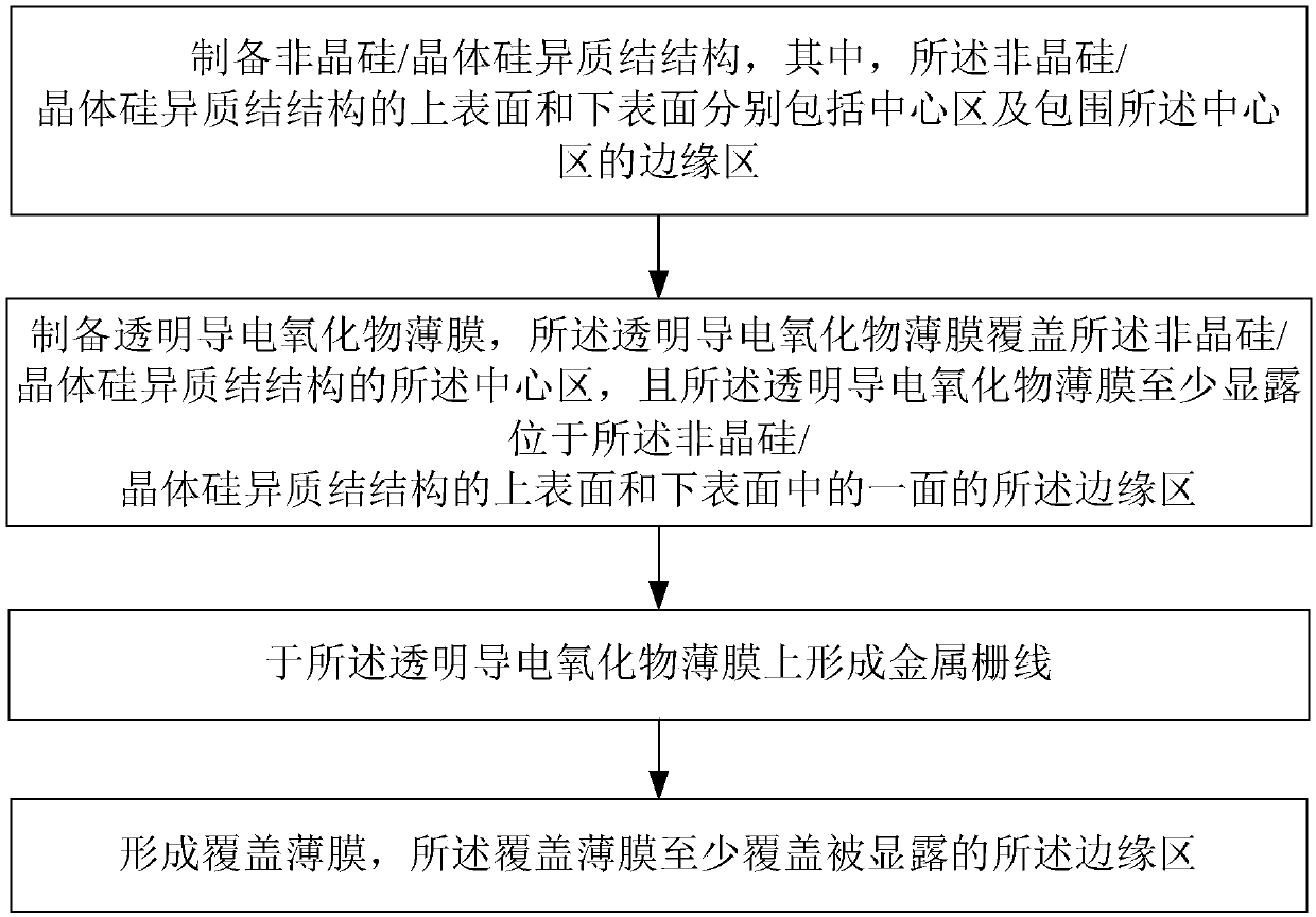
[0066] Such as figure 2 , the invention provides a method for preparing an amorphous silicon / crystalline silicon heterojunction solar cell, comprising the following steps:
[0067] preparing an amorphous silicon / crystalline silicon heterojunction structure, wherein the upper surface and the lower surface of the amorphous silicon / crystalline silicon heterojunction structure respectively include a central region and an edge region surrounding the central region;
[0068] Prepare a transparent conductive oxide film, the transparent conductive oxide film covers the central region of the amorphous silicon / crystalline silicon heterojunction structure, and the transparent conductive oxide film at least exposes the amorphous silicon / crystalline silicon heterojunction structure said edge region on one of the upper and lower surfaces of the crystalline silicon heterojunction structure;
[0069] forming a metal electrode on the transparent conductive oxide film;
[0070] A cover film ...
Embodiment 2
[0089] Figure 6a ~ Figure 6b , the present invention also provides an amorphous silicon / crystalline silicon heterojunction solar cell, the amorphous silicon / crystalline silicon heterojunction solar cell comprising:
[0090] An amorphous silicon / crystalline silicon heterojunction structure 100, the upper surface and the lower surface of the amorphous silicon / crystalline silicon heterojunction structure 100 respectively include a central region A and an edge region B surrounding the central region A;
[0091] A transparent conductive oxide film 200, the transparent conductive oxide film 200 covers the central region A of the amorphous silicon / crystalline silicon heterojunction structure 100, and the transparent conductive oxide film 200 at least exposes the The edge region B on one of the upper surface and the lower surface of the amorphous silicon / crystalline silicon heterojunction structure 100;
[0092] a metal electrode 300 located on the transparent conductive oxide film ...
PUM
| Property | Measurement | Unit |
|---|---|---|
| Thickness | aaaaa | aaaaa |
| Thickness | aaaaa | aaaaa |
| Thickness | aaaaa | aaaaa |
Abstract
Description
Claims
Application Information