N-type FET and manufacturing method thereof
A manufacturing method, N-type technology, applied in semiconductor/solid-state device manufacturing, electrical components, circuits, etc., can solve problems such as inability to further reduce device leakage and conflicts in doping control requirements, and achieve great application prospects and commercial value. Reduce subthreshold leakage current and simple process
- Summary
- Abstract
- Description
- Claims
- Application Information
AI Technical Summary
Problems solved by technology
Method used
Image

Examples
Embodiment Construction
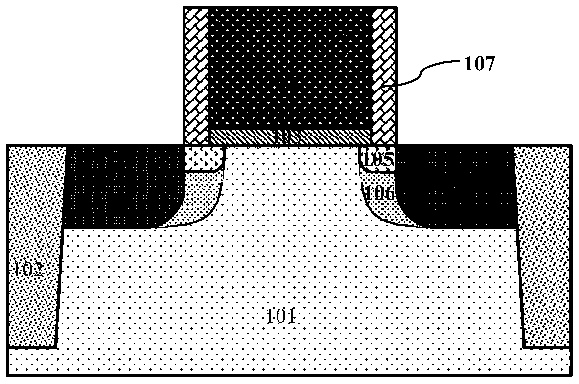
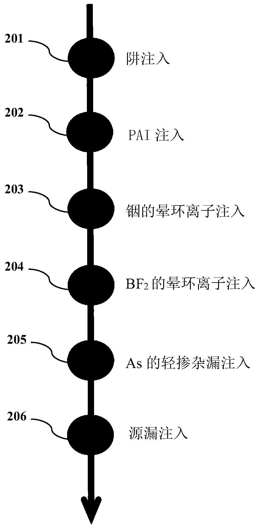
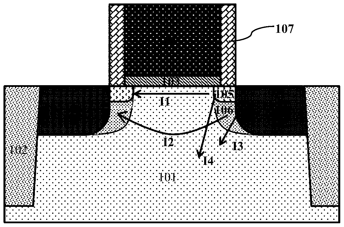
[0071] Such as Figure 4 As shown, it is a schematic diagram of the structure of the N-type FET of the embodiment of the present invention; the N-type FET of the embodiment of the present invention includes a gate structure, a spacer 7, a lightly doped drain region 5, a source region 8, a drain region 9 and a halo implantation region 6.
[0072] The gate structure is formed on the surface of the semiconductor substrate 1 . Field oxygen 2 is also formed on the semiconductor substrate 1, and the field oxygen 2 isolates an active region.
[0073] In the embodiment of the present invention, a P-type well is formed on the semiconductor substrate 1, the formation region of the NFET is located in the formation region of the P-type well, and the gate structure is formed in the P-type well On the surface.
[0074] The semiconductor substrate 1 includes a silicon substrate.
[0075] The gate structure includes a gate dielectric layer 3 and a gate conductive material layer 4 stacked ...
PUM
 Abstract
Description
Claims
Application Information
 - R&D
- Intellectual Property
- Life Sciences
- Materials
- Tech Scout
- Unparalleled Data Quality
- Higher Quality Content
- 60% Fewer Hallucinations
Browse by: Latest US Patents, China's latest patents, Technical Efficacy Thesaurus, Application Domain, Technology Topic, Popular Technical Reports.
© 2025 PatSnap. All rights reserved.Legal|Privacy policy|Modern Slavery Act Transparency Statement|Sitemap|About US| Contact US: help@patsnap.com