Quantum dot single photon source, preparation method and preparation method of device thereof

A single photon source, quantum dot technology, applied in semiconductor devices, electrical components, circuits, etc., can solve the problems of difficult operation, low external quantum efficiency, difficult batch preparation, etc., to improve the fluorescence reflectivity and reduce the production cost. , the effect of improving the utilization rate

Active Publication Date: 2020-08-11
INST OF SEMICONDUCTORS - CHINESE ACAD OF SCI
View PDF8 Cites 0 Cited by
  • Summary
  • Abstract
  • Description
  • Claims
  • Application Information

AI Technical Summary

Problems solved by technology

[0009] In the preparation process of quantum dot single photon source, not only there are problems of difficult operation, but also it is difficult to meet the practical requirements of matching with optical fiber, there are also problems of high cost and difficult batch preparation
The prepared quantum dots also have the problem of low external quantum efficiency.

Method used


Image

  • Quantum dot single photon source, preparation method and preparation method of device thereof
  • Quantum dot single photon source, preparation method and preparation method of device thereof
  • Quantum dot single photon source, preparation method and preparation method of device thereof

Examples


Embodiment 1

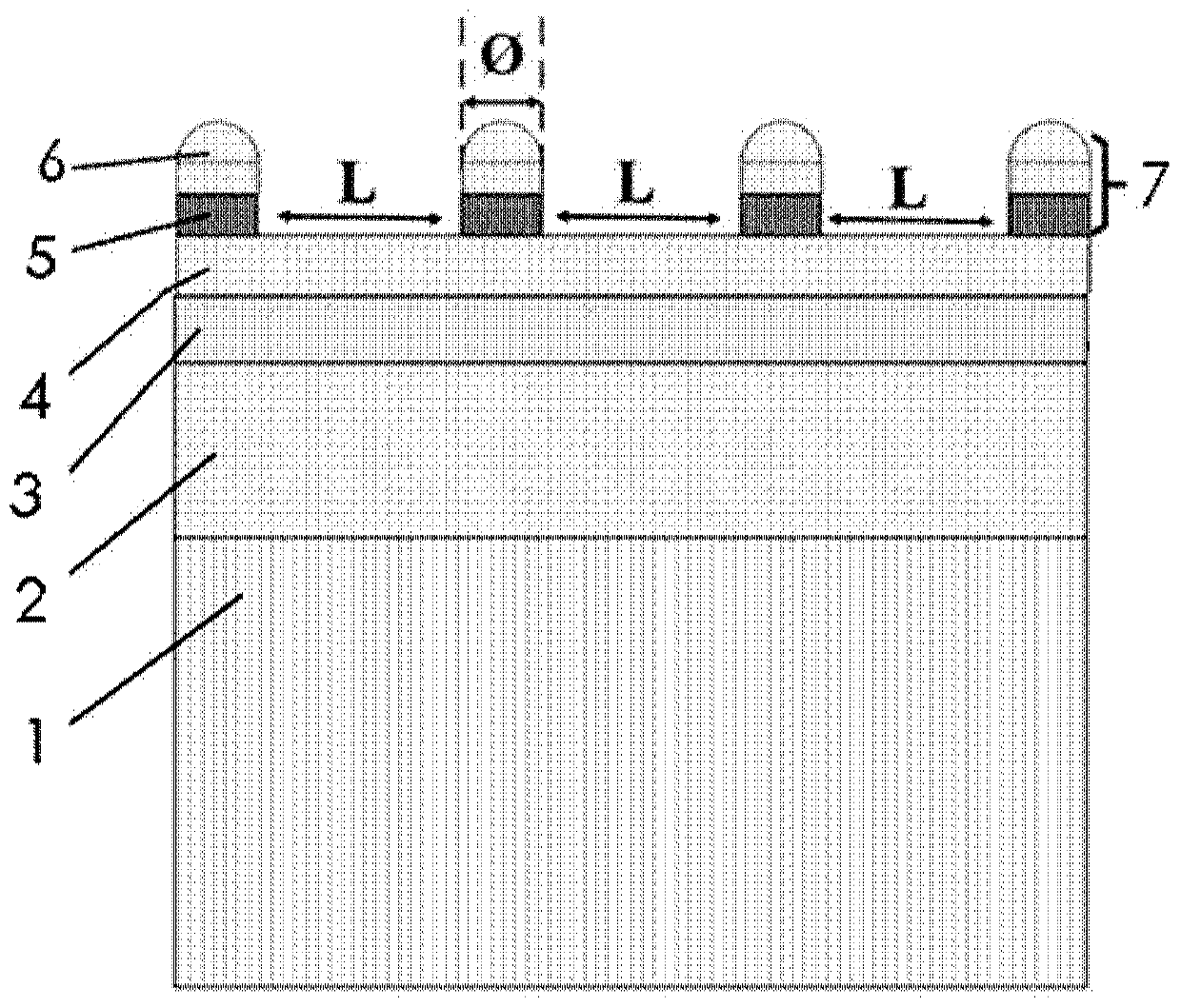
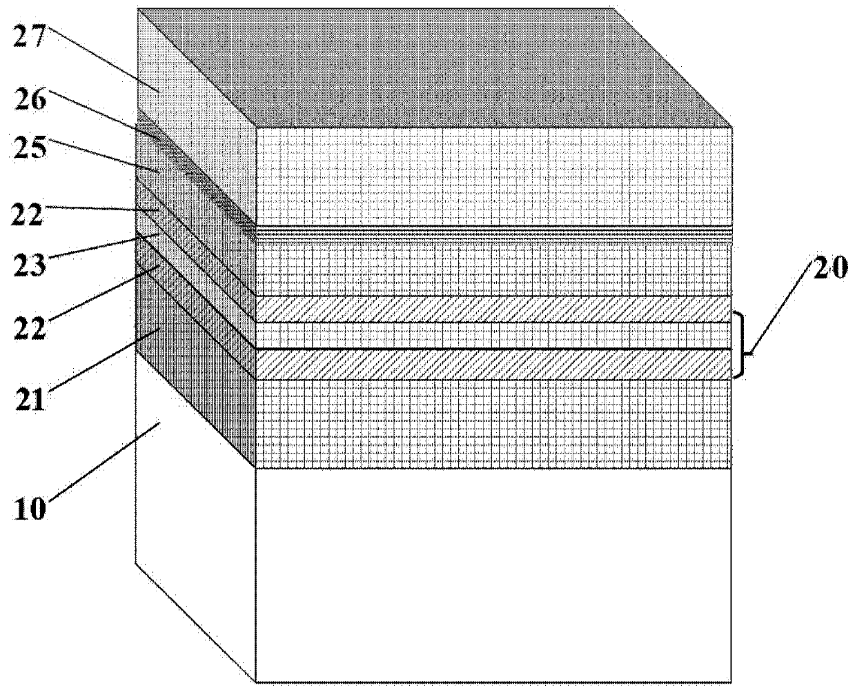
[0045] The embodiment of the present invention provides a kind of InAs / GaAs quantum dot single photon source, see image 3 and Figure 4 , the InAs / GaAs quantum dot single photon source includes:

[0046] GaAs substrate 10, GaAs buffer layer 21, DBR reflection layer 20, GaAs absorption layer 25, InAs active layer 26, GaAs capping layer 27, InAs / GaAs quantum dot array 30;

[0047] The GaAs buffer layer 21 is epitaxially grown on the GaAs substrate 10;

[0048] The DBR reflective layer 20 is epitaxial on the GaAs buffer layer 21;

[0049] The GaAs absorption layer 25 is epitaxial on the DBR reflective layer 20;

[0050] The InAs active layer 26 is epitaxy on the GaAs absorbing layer 25;

[0051] The GaAs capping layer 27 is epitaxially grown on the InAs active layer 26;

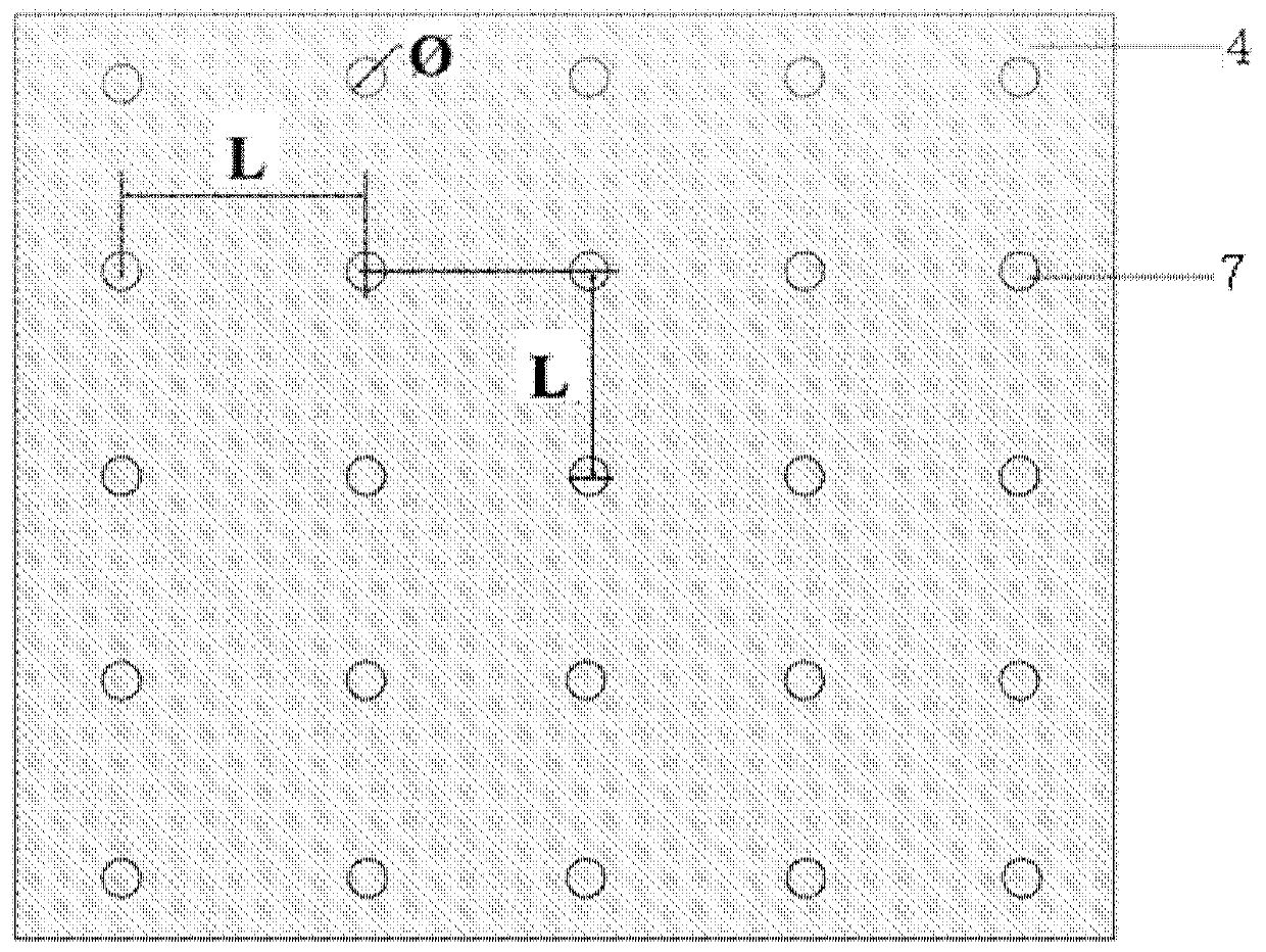
[0052] The InAs / GaAs quantum dot array 30 is located on the GaAs absorbing layer 25 by etching the GaAs capping layer 27 and the InAs active layer 26 .

[0053] Wherein, the DBR reflective layer 20 refers...

Embodiment 2

[0074] The embodiment of the present invention provides an InSb / GaAs quantum dot single photon source and a preparation method thereof, and a preparation method of an InSb / GaAs quantum dot single photon source device.

[0075] The difference between the InSb / GaAs quantum dot single photon source provided in this embodiment and the first embodiment is that an InSb active layer is disposed on a GaAs absorption layer in this embodiment. That is, the InAs active layer in the first embodiment is replaced with an InSb active layer. The InSb / GaAs quantum dot single photon source is obtained by etching the active layer and the cover layer. This embodiment contains a DBR reflective layer.

[0076] At room temperature of 300K, the intrinsic electron concentration of InSb material is 2×10 16 cm -3 , the electron mobility can reach 7×10 4 cm 2 V -1 the s -1 , therefore, InSb material is naturally a natural candidate material for preparing excellent quantum dots.

[0077] The InSb ...

Embodiment 3

[0083] The embodiment of the present invention provides a GaSb / GaAs quantum dot single photon source and a preparation method thereof, and a preparation method of a GaSb / GaAs quantum dot single photon source device.

[0084] The difference between the GaSb / GaAs quantum dot single photon source provided in this embodiment and the first embodiment is that the GaSb active layer is disposed on the GaAs absorption layer in this embodiment. That is, the InAs active layer in the first embodiment is replaced with a GaSb active layer. The GaSb / GaAs quantum dot single photon source is obtained by etching the active layer and the cover layer. This embodiment contains a DBR reflective layer.

[0085] Wherein, the thickness of the GaSb active layer is 0.5 nm. The GaSb active layer is δ-doped, using n-type GaTe doping with a doping concentration of 2E18cm -3 .

[0086] In the preparation method of the GaSb / GaAs quantum dot single photon source, the difference between this embodiment and...


PUM

PropertyMeasurementUnit
diameteraaaaaaaaaa
heightaaaaaaaaaa
thicknessaaaaaaaaaa

Abstract

The invention provides a quantum dot single photon source and a preparation method thereof, and a preparation method of a device of the quantum dot single photon source. The quantum dot single photonsource comprises a substrate, a buffer layer, and / or a DBR reflection layer, an absorption layer, an active layer, a cover layer, and a quantum dot array, wherein the buffer layer is arranged on the substrate, the DBR reflection layer is arranged on the buffer layer, the absorption layer is arranged on the DBR reflection layer, the active layer is arranged on the absorption layer, the cover layeris arranged on the active layer, the quantum dot array is obtained by etching the cover layer and the active layer, and the quantum dot array is located on the absorption layer. The fluorescence emissivity of the quantum dot single-photon source device is improved, and the yield of the manufactured quantum dot single-photon source device is improved.

Description

technical field [0001] The invention relates to the technical field of semiconductor materials and devices, in particular to a quantum dot single photon source, a preparation method and a preparation method for devices thereof. Background technique [0002] Quantum dot single photon source refers to a single two-level system that emits a single fixed-frequency photon at regular intervals under the excitation of optical or electrical pumping. High-quality quantum dot single-photon sources have broad application prospects in quantum computing, quantum communication, quantum measurement, and quantum storage. [0003] The solid semiconductor quantum dots produced by molecular beam epitaxy technology not only finally realize the three-dimensional confinement of carriers, but also lead to the quantization of carrier energy in three dimensions and have discrete energy levels, presenting an "atom-like" shell fill properties. People have observed the anti-bunching effect of photo-i...

Claims


Application Information

Patent Timeline
Patent Type & Authority Applications(China)
IPC IPC(8): H01L33/06H01L33/30H01L33/10H01L33/00
CPCH01L33/0062H01L33/06H01L33/10H01L33/30
Inventor 何小武牛智川张宇徐应强陈昊孙宝权窦秀明尚向军倪海桥任正伟刘汗青
Owner INST OF SEMICONDUCTORS - CHINESE ACAD OF SCI
Why Eureka
Try Eureka