Photon information processing chip

A photonic signal and chip technology, applied in the direction of electrical digital data processing, architecture with a single central processing unit, physical realization, etc., can solve problems such as expensive maintenance systems, achieve information processing energy consumption reduction, information processing time reduction, information Effect of processing capacity improvement

Active Publication Date: 2020-08-14
OTN INTELLIGENT TECH (SUZHOU) CO LTD
View PDF7 Cites 1 Cited by
  • Summary
  • Abstract
  • Description
  • Claims
  • Application Information

AI Technical Summary

Problems solved by technology

However, current quantum computers require extremely expensive maintenance systems, such as liquid nitrogen ultra-low temperature cooling systems, etc., and cannot achieve super computing power at low cost

Method used


Image

  • Photon information processing chip
  • Photon information processing chip
  • Photon information processing chip

Examples


Embodiment 1

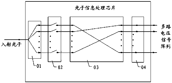
[0032] Embodiment 1 Photonic digital processor chip

[0033] Such asfigure 1 and figure 2 As shown, the parallel beam expander unit 01 divides the incident photon wave, whose wavelength range is 1500nm-1600nm, into multiple specific channels according to different wavelengths, and sets the number of specific channels as n to form n beams of photons. In this embodiment, n=50 A specific channel can be achieved through a grating. In order to make the manufacturing process of the parallel beam expander unit 01 compatible with the silicon-based chip processing technology, the silicon substrate can be doped with nitrogen and oxygen by magnetron sputtering, so that the optical loss of the photon beam in its optical waveguide is less than 0.5 dB / cm, in order to realize the propagation of a specific wavelength along a specific channel through the interference effect of light, the width interval between the optical waveguides of adjacent different channels must be precisely controlled...

Embodiment 2

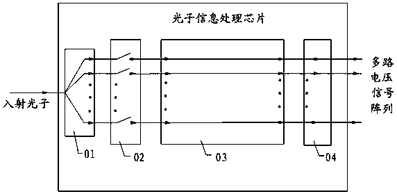
[0037] Embodiment 2 photonic artificial intelligence operation chip

[0038] Such as figure 1 and image 3 As shown, the parallel beam expander unit 01 divides the incident photon wave, whose wavelength range is 1500nm-1600nm, into n specific channels according to different wavelengths, and sets the number of specific channels as n to form n beams of photons. In this embodiment, n=50 For a specific channel, in order to make the manufacturing process of the parallel beam expander unit 01 compatible with the silicon-based chip processing technology, we doped nitrogen and oxygen on the silicon substrate by magnetron sputtering, so that the photon beam in its optical waveguide The optical loss is less than 0.5dB / cm; in order to realize the propagation of a specific wavelength along a specific channel through the interference effect of light, the width interval between the optical waveguides of adjacent different channels must be precisely controlled, that is, the precision d of l...


PUM

PropertyMeasurementUnit
wavelengthaaaaaaaaaa

Abstract

The invention discloses a photon information processing chip, and the photon information processing chip comprises: a parallel beam expanding unit which is used for dividing an input photon signal into a plurality of photon signals according to different wavelength intervals, so as to achieve the parallel information processing; the weight setting unit which is used for setting weight values of different levels for the intensity values or the phase values of the photon beams with different wavelength intervals behind the parallel beam expanding unit; the crossover operation unit which is usedfor reallocating propagation channels to the photon beams which are set to be different in weight value after the weight setting unit according to different control voltage values; and the photoelectric receiving array which is used for converting each photon beam with different wavelength intervals into a multi-path voltage signal array through photoelectricity after the propagation channels areredistributed by the crossover operation unit, and the four units are manufactured on the same silicon-based material. Therefore, by utilizing the photon information processing chip provided by the invention, the information processing capacity is greatly improved, the information processing time is greatly reduced, and the information processing energy consumption is greatly reduced.

Description

technical field [0001] The invention relates to the field of chip technology, in particular to a photonic information processing chip. Background technique [0002] Information processing technology is the basic core technology of the current information age. Artificial intelligence, big data, image recognition and other fields need to process massive amounts of digital or analog information, so they need super-powerful information processing technology to support them. [0003] So far, the information processing technology used by people is basically based on electronic information processing technology, among which highly integrated digital electronic computers are the mainstream. However, no matter in the field of artificial intelligence, big data or image recognition, people have gradually realized that the current computer technology has been overwhelmed. [0004] Based on the fact that the current electronic information processing technology can hardly meet the needs...

Claims


Application Information

Patent Timeline
Patent Type & Authority Applications(China)
IPC IPC(8): G06E1/00G06F15/78G06N3/067
CPCG06E1/00G06F15/7807G06N3/0675Y02D10/00
Inventor 周炆杰刘晓海
Owner OTN INTELLIGENT TECH (SUZHOU) CO LTD
Why Eureka
Try Eureka