Packaging structure of multi-chip wide bandgap power module based on conductive metal clip interconnection

A conductive metal and power module technology, applied in circuits, electrical components, semiconductor devices, etc., can solve the problems of reducing the service life of power modules, increasing the volume of power modules, and accelerating the failure of power modules, so as to reduce the possibility of failure, The effect of reducing module size and improving reliability

Active Publication Date: 2021-08-13
XI AN JIAOTONG UNIV
View PDF6 Cites 0 Cited by
  • Summary
  • Abstract
  • Description
  • Claims
  • Application Information

AI Technical Summary

Problems solved by technology

[0005] 2. Traditional power modules mostly use aluminum bonding wires as the interconnection method in electrical connection, which is characterized by one-sided heat transfer. This heat dissipation method is called single-sided heat dissipation, and the heat dissipation efficiency is low. High resistance, which is very unfavorable for the use of power modules in harsh environments; aluminum bonding wires are prone to aging or even falling off at the bonding points under high temperature applications, resulting in failure of power modules, which is not conducive to the application of power modules in extreme environments; The flow area of ​​the aluminum bonding wire is small, and the current passing through one bonding wire is limited. In the power module that needs to pass a large current, more than 20 bonding wires need to be used, which makes the power module The process is complicated, and the volume of the power module is also increased due to insufficient space utilization;
[0006] 3. It is difficult for traditional power modules to achieve chip current sharing and temperature sharing, which is crucial in high operating frequency and harsh environments
The uneven dynamic current of the chip is mainly due to the uneven distribution of the parasitic inductance of the parallel branch of the chip. The uneven distribution of the parasitic inductance will cause the power chip to be subjected to unequal current and voltage stress during the switching transient, and the breakdown of the power chip is very likely to occur. Ineffectiveness, which has a more obvious impact on wide-bandgap semiconductor power devices; at the same time, uneven dynamic current can cause uneven chip loss, which in turn makes chip temperature uneven, resulting in aging and failure of the bonding layer of different chips The rate is different, and by affecting the threshold voltage of the chip, it will aggravate the dynamic current unevenness of the parallel chip, and further accelerate the failure of the power module as a whole
[0007] Some companies use copper sheets instead of traditional bonded aluminum wires to complete the interconnection of power semiconductors, but the shape of the connection parts has not been specially designed, resulting in greater stress on the copper sheets and solder layers under working conditions, reducing power The service life of the module; in addition, this method is currently only used for the connection of single-power chips, which cannot meet the requirements of high-power and high-current applications.

Method used


Image

  • Packaging structure of multi-chip wide bandgap power module based on conductive metal clip interconnection
  • Packaging structure of multi-chip wide bandgap power module based on conductive metal clip interconnection
  • Packaging structure of multi-chip wide bandgap power module based on conductive metal clip interconnection

Examples


Embodiment

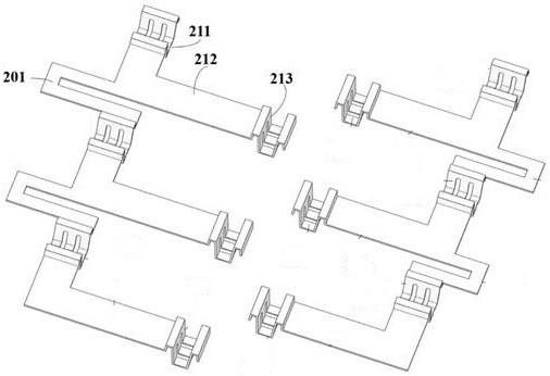
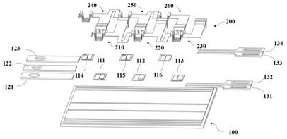
[0061] see figure 1 , figure 2 and image 3 , the packaging structure of this embodiment is mainly composed of 6 power electronic power semiconductor chips, 3 power substrates, 3 power terminals, 4 drive terminals and 2 conductive metal clips;

[0062] The six power electronic power semiconductor chips are specifically a semiconductor chip 111, a semiconductor chip 112, a semiconductor chip 113, a semiconductor chip 114, a semiconductor chip 115, and a semiconductor chip 116;

[0063] The three power substrates are specifically the lower surface conductive metal substrate 108, the insulating dielectric substrate 109 and the upper surface conductive metal substrate;

[0064] The three power terminals are specifically DC power terminal positive pole 121, DC power terminal negative pole 122 and AC power terminal 123;

[0065] The four drive terminals are specifically the source drive terminal 131 of the upper arm using the Kelvin connection method, the gate drive terminal 132...


PUM


Abstract

The invention discloses a multi-chip wide bandgap power module packaging structure based on the interconnection of conductive metal clips, including power substrates, conductive metal clips, power terminals, drive terminals and electronic power semiconductor chips, suitable for multiple wide High-current level power modules with band-gap semiconductor power chips connected in parallel. A number of series or parallel power electronic power semiconductor chips are arranged on the conductive metal substrate on the upper surface of the power substrate; in the power circuit, a conductive metal clip is used to replace the traditional aluminum bonding wire to complete the electrical connection of the power circuit in the power module; the conductive metal The layout design of the clip greatly improves the distribution uniformity of the parasitic inductance of the parallel branch in the power module, achieving the effect of parallel chip current sharing; the same spacing between adjacent chips ensures that the heat dissipation conditions are almost the same, achieving the effect of chip temperature uniformity; The shape design of the conductive metal clip connector reduces the thermal-mechanical stress generated by the work and improves the reliability of the power module; the heat transfer capability of the conductive metal clip enables the power module to achieve a double-sided heat dissipation structure.

Description

technical field [0001] The invention belongs to the technical field of semiconductor packaging, and in particular relates to a multi-chip wide bandgap power module packaging structure based on conductive metal clip interconnection. Background technique [0002] The power module is a module formed by packaging and integrating a series of power electronic power chips according to certain functions. Compared with the power electronic converter composed of discrete power electronic power devices, the power module has high reliability and high integration It has high advantages in electrical performance, thermal performance, safety protection, cost and so on. [0003] In recent years, with the continuous development of power electronic devices, the continuous improvement of application environment requirements in important fields such as oil drilling, electric vehicles, shipboard systems, and aerospace, and the introduction of energy-saving slogans, power modules are moving to sm...

Claims


Application Information

Patent Timeline
Patent Type & Authority Patents(China)
IPC IPC(8): H01L25/065H01L23/48H01L23/14H01L23/367
CPCH01L23/142H01L23/367H01L23/48H01L24/72H01L25/0655H01L2224/72
Inventor 王来利张彤宇杨奉涛
Owner XI AN JIAOTONG UNIV
Why Eureka
Try Eureka