Mid-far infrared avalanche photodetector

An avalanche photoelectric and detector technology, applied in circuits, electrical components, semiconductor devices, etc., can solve the problems of inconvenient use, low carrier concentration, increased cost, etc., achieve room temperature operation, reduce device noise, and improve device performance. performance effect

Inactive Publication Date: 2020-08-14
INST OF SEMICONDUCTORS - CHINESE ACAD OF SCI
View PDF7 Cites 3 Cited by
  • Summary
  • Abstract
  • Description
  • Claims
  • Application Information

AI Technical Summary

Problems solved by technology

At present, commercial mid-to-far infrared detectors are mainly made of mercury cadmium telluride, but mercury cadmium telluride avalanche photodetectors need to work at low temperatures, which increases the cost of low temperature configuration and is inconvenient to use
In addition, pure InAs avalanche photodetectors, which are currently researched more, need to epitaxially grow thicker InAs materials in order to obtain high gain, which increases the cost. At the same time, it is necessary to ensure that the carrier concentration in this layer of material is low, at 10 14 cm -3 magnitude, which poses a huge challenge to epitaxial growth

Method used


Image

  • Mid-far infrared avalanche photodetector

Examples


Embodiment Construction

[0035] In order to make the object, technical solution and advantages of the present invention clearer, the present invention will be further described in detail below in conjunction with specific embodiments and with reference to the accompanying drawings.

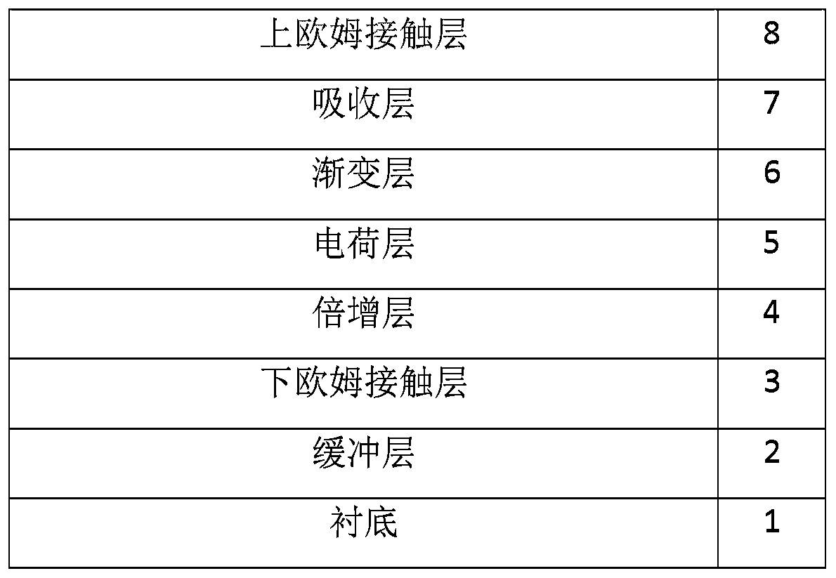
[0036] Based on the antimonide semiconductor compound family system, the present invention provides a mid-to-far infrared avalanche photodetector, including:

[0037] Substrate 1, buffer layer 2, lower ohmic contact layer 3, multiplication layer 4, charge layer 5, gradient layer 6, absorption layer 7 and upper ohmic contact layer 8 connected in sequence from bottom to top, and substrate 1 and buffer layer The doping type of 2 is n-type; or

[0038] The substrate 1, the buffer layer 2, the second ohmic contact layer 8, the absorption layer 7, the graded layer 6, the charge layer 5, the multiplication layer 4 and the first ohmic contact layer 3 are sequentially connected from bottom to top, and the substrate The doping typ...


PUM

PropertyMeasurementUnit
thicknessaaaaaaaaaa
thicknessaaaaaaaaaa
thicknessaaaaaaaaaa

Abstract

The invention discloses a mid-far infrared avalanche photodetector which comprises a substrate, a buffer layer, a lower ohmic contact layer, a multiplication layer, a charge layer, a gradient layer, an absorption layer and an upper ohmic contact layer which are sequentially connected from bottom to top, and the doping type of the substrate and the buffer layer is n type. Or the mid-far infrared avalanche photodetector comprises the substrate, the buffer layer, a second ohmic contact layer, the absorption layer, the gradient layer, the charge layer, the multiplication layer and a first ohmic contact layer which are sequentially connected from bottom to top, and the doping type of the substrate and the buffer layer is p type, wherein the multiplication layer is made of an AlAsxSb1-x material, x is greater than or equal to 0.12 and less than or equal to 0.18, the gradient layer is of a plurality of (InAs)m/(AlAs0.15Sb0.85)n quantum well structures or an InyAl1-yAszSb1-z material, and thedetection wavelength of the absorption layer is a middle and far infrared band. The mid-far infrared avalanche photodetector provided by the invention can block dark current and reduce noise, does notneed a cooling device, improves the working temperature of the device, reduces the cost, and is convenient to use.

Description

technical field [0001] The invention relates to the technical field of semiconductors, in particular to a mid-far infrared avalanche photodetector with a wavelength greater than 3.0 microns. Background technique [0002] Mid-to-far infrared avalanche photodetectors have very important applications in both military and civilian fields, such as night vision, early warning, environmental monitoring, single photon detection and free communication. At present, commercial mid-to-far infrared detectors are mainly made of mercury cadmium telluride, but mercury cadmium telluride avalanche photodetectors need to work at low temperatures, which increases the cost of low temperature configuration and is inconvenient to use. In addition, pure InAs avalanche photodetectors, which are currently researched more, need to epitaxially grow thicker InAs materials in order to obtain high gain, which increases the cost. At the same time, it is necessary to ensure that the carrier concentration in...

Claims


Application Information

Patent Timeline
Patent Type & Authority Applications(China)
IPC IPC(8): H01L31/0304H01L31/0352H01L31/107
CPCH01L31/107H01L31/1075H01L31/035236H01L31/0304
Inventor 黄建亮马文全
Owner INST OF SEMICONDUCTORS - CHINESE ACAD OF SCI
Why Eureka
Try Eureka