Manufacturing method of deep ultraviolet LED chip with vertical structure

A technology of LED chips and manufacturing methods, applied in semiconductor devices, electrical components, circuits, etc., can solve the problems of low optical output power and external quantum efficiency, long propagation path, and affecting TM polarized light propagation, and reduce the source area. Loss, good ohmic contact performance, effect of improving light extraction efficiency

Active Publication Date: 2020-08-28
JIANGXI ZHAO CHI SEMICON CO LTD
View PDF4 Cites 7 Cited by
  • Summary
  • Abstract
  • Description
  • Claims
  • Application Information

AI Technical Summary

Problems solved by technology

[0005] Although deep UV LEDs are more cost-effective and environmentally friendly than UV lamps, they cannot easily replace UV lamps due to their low light output
Due to the low light extraction efficiency (LEE) and high epitaxial crystal defects in AlGaN-based deep ultraviolet LED chips, their light output power and external quantum efficiency (EQE) are low
As the emission wavelength decreases, the transverse magnetic (TM) polarized light propagating parallel to the c-plane of sapphire accounts for the main part, and the propagation path from the multi-quantum well is longer, and the light loss is larger, resulting in a decrease in light extraction efficiency, and at the same time, the high resistance The AlGaN layer and the current crowding phenomenon caused by the tilt angle inside the chip will also affect the propagation of TM polarized light

Method used


Image

  • Manufacturing method of deep ultraviolet LED chip with vertical structure
  • Manufacturing method of deep ultraviolet LED chip with vertical structure
  • Manufacturing method of deep ultraviolet LED chip with vertical structure

Examples


Embodiment 1

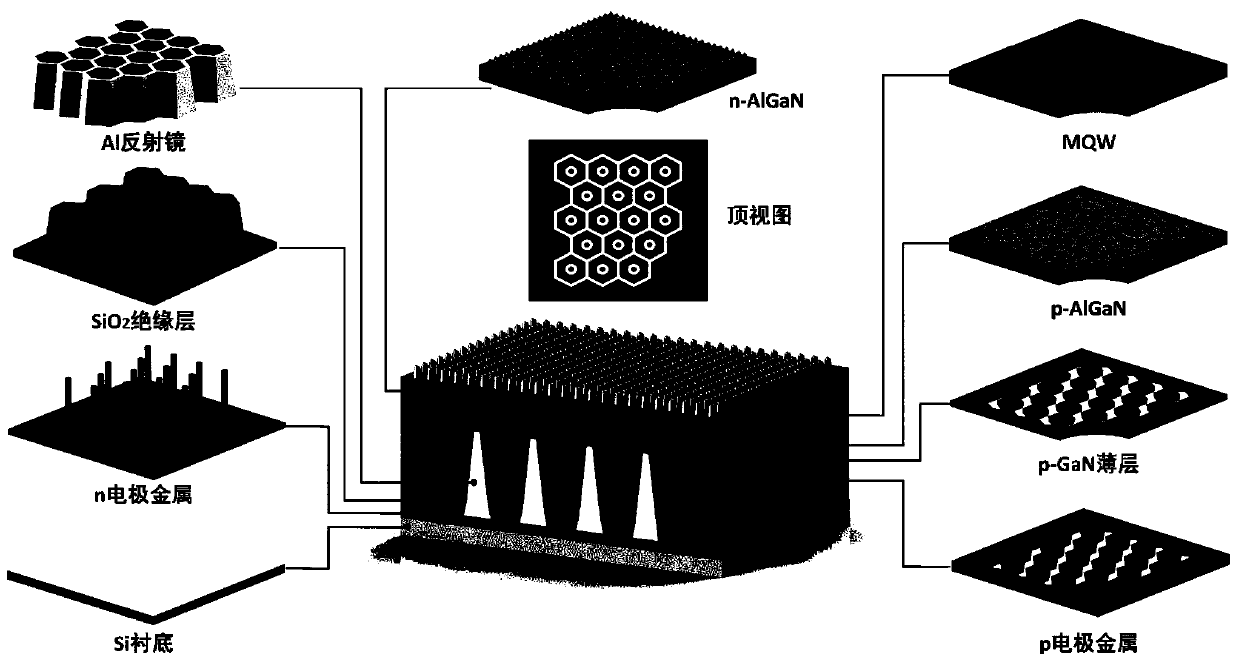
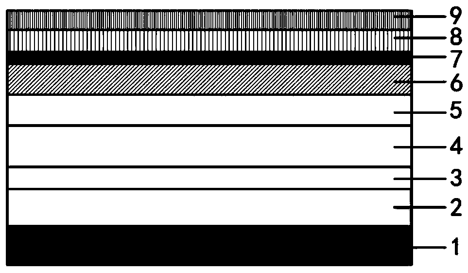
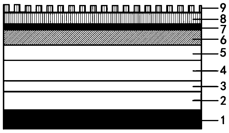
[0064] A method for manufacturing a vertical structure deep ultraviolet LED chip is provided, and the specific steps are as follows:

[0065] (1) Put the cleaned sapphire substrate 1 into the MOCVD epitaxial growth device 1 at a temperature of 650°C, and grow a 35nm AlN nucleation layer 2 .

[0066] (2) At a temperature of 1100°C, continue to grow undoped Al 0.45 Ga 0.55 N buffer layer 3 with a thickness of 175-225nm, keep the temperature constant, and grow a layer of Si-doped n-Al 0.7 Ga 0.3 N layer 4 and n-Al 0.6 Ga 0.4 N layer 5 with a thickness of 2.5 μm and 0.5 μm and a doping concentration of 1.6×10 19 cm -3 .

[0067] (3) At a temperature of 760°C, grow Al for 5 cycles 0.4 Ga 0.6 N / Al 0.64 Ga 0.36 The quantum well is used as the active layer 6, and the thickness of the quantum well layer is about 2.7nm.

[0068] (4) Deposit SiO at low temperature 2 or Si 3 N 4 Material electron blocking layer 7 (EBL), and then use the electron beam evaporation method to e...


PUM

PropertyMeasurementUnit
widthaaaaaaaaaa
lengthaaaaaaaaaa
diameteraaaaaaaaaa

Abstract

The invention discloses a manufacturing method of a deep ultraviolet LED chip with a vertical structure. The method is specifically characterized in that a p-GaN ohmic contact layer is processed intoa grid-shaped structure by using a laser direct writing process, and a p type low-resistance ohmic contact Ni / Al electrode with high reflectivity is used for ohmic contact with the p-GaN grid to formgood ohmic contact; a groove array and an inner reflector groove array are etched between a Ni / Al p electrode conductive layer and the n-AlGaN layer of an epitaxial layer to obtain a honeycomb structure, and the Al layer as a reflector is deposited on the side wall of the inner reflector groove to obtain a honeycomb-shaped inner reflector structure; and by replacing a p-GaN layer in a traditionaldeep ultraviolet LED with the grid-shaped transparent p-GaN layer and designing the honeycomb-shaped inner reflector structure, emission of photons transversely propagated on the LED active layer is achieved, loss of a source region in the deep ultraviolet LED chip is reduced, and the light extraction efficiency of the chip is greatly improved.

Description

technical field [0001] The invention belongs to the technical field of semiconductor light emitting devices, in particular to a method for manufacturing a vertical structure deep ultraviolet LED chip. Background technique [0002] As a new type of high-efficiency solid-state light source, light-emitting diodes (Light Emitting Diodes, referred to as "LED") are widely used in solid-state lighting, transportation, military and medical fields due to their high efficiency, long life, energy saving, environmental protection, and rich colors. . With the gradual maturity of LED technology and the needs of industrialization and marketization, there are stricter requirements on the luminous efficiency and other properties of LED devices. As a branch of LED, ultraviolet LED can not illuminate but has all the advantages of LED. In theory, it can replace all traditional ultraviolet light sources, which greatly expands the application field of LED. The most common ultraviolet rays mainl...

Claims


Application Information

Patent Timeline
Patent Type & Authority Applications(China)
IPC IPC(8): H01L33/32H01L33/06H01L33/14H01L33/00H01L33/20
CPCH01L33/0075H01L33/06H01L33/14H01L33/20H01L33/32
Inventor 周圣军徐浩浩万泽洪
Owner JIANGXI ZHAO CHI SEMICON CO LTD
Why Eureka
Try Eureka