Electron-hole reversible doping method of multilayer molybdenum ditelluride field effect transistor

A field-effect transistor and molybdenum ditelluride field technology, which is applied in the control field of electron transport performance transformation, can solve the problems of complex control methods, small control range, and limited tuning range, and achieve simple and convenient process and operating conditions, and high-quality materials. Less damage, environment-friendly effect

Active Publication Date: 2020-09-04
WENZHOU UNIVERSITY
View PDF6 Cites 1 Cited by
  • Summary
  • Abstract
  • Description
  • Claims
  • Application Information

AI Technical Summary

Problems solved by technology

However, these methods are either complicated or have limited tuning range, and the manufacturing process of the device, such as the aforementioned ultraviolet light irradiation, may also change the MoTe 2 crystal structure, which greatly affects the MoTe 2 electron transport properties
[0005] In short, there are certain limitations in the methods for adjusting the electron transport characteristics of molybdenum ditelluride devices in the prior art: either one-way N-type or P-type doping adjustment for electron transport properties, or the regulation method is complicated Or the control range is small and the degree is low, and it is possible to change the MoTe 2 Structure

Method used


Image

  • Electron-hole reversible doping method of multilayer molybdenum ditelluride field effect transistor
  • Electron-hole reversible doping method of multilayer molybdenum ditelluride field effect transistor
  • Electron-hole reversible doping method of multilayer molybdenum ditelluride field effect transistor

Examples


Embodiment 1 2

[0034] Embodiment 1 Electron-hole reversible doping of molybdenum ditelluride field effect transistor

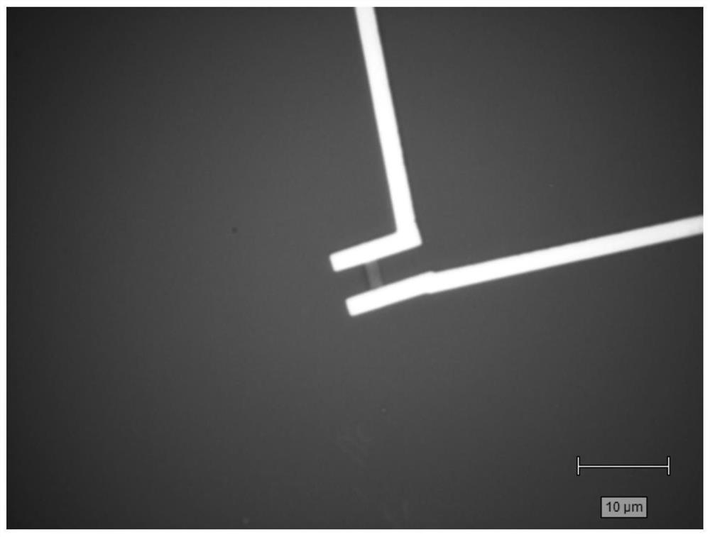
[0035] (1)MoTe 2 Fabrication of Field Effect Transistor Devices:

[0036] By mechanical exfoliation, the bulk MoTe 2 The layered crystals are placed on the tape, and the tape is pasted and torn repeatedly; the MoTe 2 A thin layer of adhesive tape is pressed on the polydimethylsiloxane (PDMS, polydimethylsiloxane) film. Due to the stickiness on the surface of the PDMS film, a small amount of MoTe 2 The thin layer was transferred onto the PDMS membrane; the clean surface layer was 300nm of SiO 2 silicon wafer (denoted as SiO 2 / Si substrate) pressed onto the PDMS film, then there will be a small amount of MoTe 2 Thin layer transfer to SiO 2 / SiO in Si substrate 2 on the surface of the layer;

[0037] Observation of SiO under an optical microscope 2 / Si substrate, determined thin layer MoTe 2 The position of the crystal; spin coating at this position (the first time: ...

Embodiment 2 2

[0044] Embodiment 2 Electron-hole reversible doping of molybdenum ditelluride field effect transistor

[0045] Basically the same as embodiment 1, the difference is only that step (2) takes the following method:

[0046] (2)MoTe 2 P-type doping (hole doping) of field effect transistor devices:

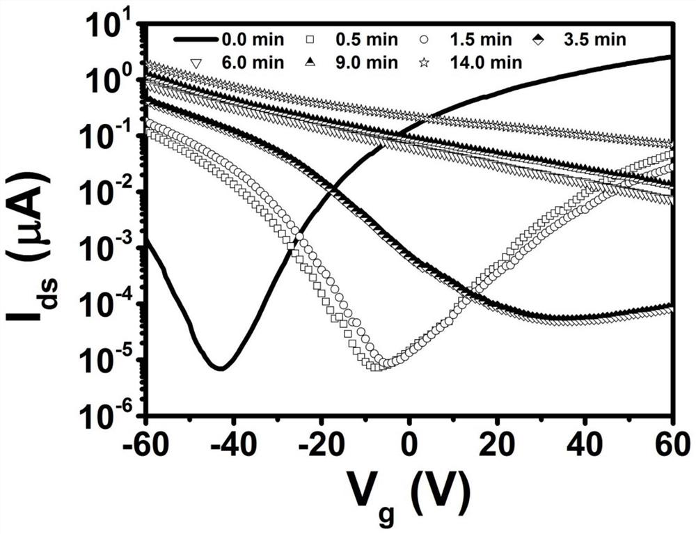
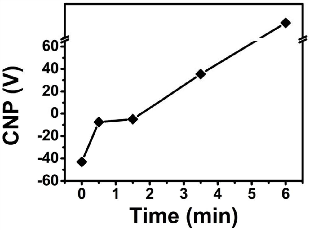
[0047] The MoTe prepared by step (1) 2 The field effect transistor device is placed on a heating platform that has been preheated to the target heating temperature, and the target heating temperature is maintained and heated in the air for 1.5min. The target heating temperature is 423K, and P-type doped MoTe is obtained. 2 field effect transistor devices. After the obtained device was cooled to room temperature, the electrical performance test was carried out in air.

Embodiment 3 2

[0048] Embodiment 3 Electron-hole reversible doping of molybdenum ditelluride field effect transistor

[0049] (1)MoTe 2 Fabrication of Field Effect Transistor Devices:

[0050] By mechanical exfoliation, the bulk MoTe 2 The layered crystals are placed on the tape, and the tape is pasted and torn repeatedly; the MoTe 2 A thin layer of adhesive tape is pressed on the polydimethylsiloxane (PDMS, polydimethylsiloxane) film. Due to the stickiness on the surface of the PDMS film, a small amount of MoTe 2 The thin layer was transferred onto the PDMS membrane; the clean surface layer was 300nm of SiO 2 silicon wafer (denoted as SiO 2 / Si substrate) pressed onto the PDMS film, then there will be a small amount of MoTe 2 Thin layer transfer to SiO 2 / SiO in Si substrate 2 on the surface of the layer;

[0051] Observation of SiO under an optical microscope 2 / Si substrate, determined thin layer MoTe 2 The position of the crystal; spin coating at this position (the first time: ...


PUM

PropertyMeasurementUnit
thicknessaaaaaaaaaa
thicknessaaaaaaaaaa
thicknessaaaaaaaaaa

Abstract

The invention discloses an electron-hole reversible doping method of a multilayer molybdenum telluride field effect transistor. The method comprises the following steps of: preparing a MoTe2 field effect transistor device by using a mechanical stripping method; then heating the MoTe2 field effect transistor device in air at a proper temperature for a proper time to obtain a P-type doped MoTe2 field effect transistor device; and irradiating the surface of the MoTe2 field effect transistor by using a high-voltage electron beam in a scanning electron microscope cabin to obtain the N-type doped MoTe2 field effect transistor device. The P-type doping process and the N-type doping process can be repeated and controllable. The electron-hole reversible doping method of the multi-layer molybdenum ditelluride field effect transistor is realized, so that the electron transport polarity of a molybdenum ditelluride device can be controlled in a large range, and the method is simple, good in repeatability, good in measured molybdenum ditelluride performance, small in damage to materials, simple in required condition and environmentally friendly.

Description

technical field [0001] The invention belongs to the technical field of inorganic nanometer materials and microelectronics, and specifically relates to MoTe 2 A control method for the transition of electron transport properties. Background technique [0002] A two-dimensional material is a layered material that has only a single or multiple atomic layers in the thickness direction and is stacked by van der Waals forces between layers. Two-dimensional materials have the following advantages: they have an atomic-level thickness, so that the charge carrier concentration and photoelectric properties can be effectively regulated by local electric fields and other means; the band gap is distributed between 0-6eV, and a wide range Electromagnetic spectral response; there is a weak van der Waals force between layers, without considering the limitation of lattice matching, so as to meet different needs and device applications. Therefore, the application of two-dimensional layered co...

Claims


Application Information

Patent Timeline
Patent Type & Authority Applications(China)
IPC IPC(8): H01L21/383H01L21/423H01L21/428H01L21/34
CPCH01L29/66969H01L21/383H01L21/423H01L21/428
Inventor 张礼杰罗婷燕潘宝俊董幼青邹超
Owner WENZHOU UNIVERSITY
Why Eureka
Try Eureka