Diamond wire for cutting large-size photovoltaic silicon wafer and manufacturing method thereof
A manufacturing method and diamond wire technology, applied in the direction of manufacturing tools, final product manufacturing, sustainable manufacturing/processing, etc., can solve problems such as increased TTV defect ratio, reduce the probability of micro-powder adhesion and agglomeration, improve performance, and increase toughness and strength Effect
- Summary
- Abstract
- Description
- Claims
- Application Information
AI Technical Summary
Problems solved by technology
Method used
Image

Examples
Embodiment 1
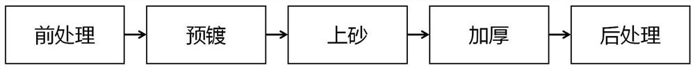
[0049] like figure 1As shown, this embodiment provides a manufacturing method of diamond wire for cutting photovoltaic large-size silicon wafers, which includes the following steps: (1) pretreatment, processing the diamond fine powder and the busbar; (2) preplating, electroplating on the surface of the busbar A layer of nickel coating; (3) Sanding, using the principle of composite electroplating to fix the diamond powder on the busbar; (4) Thickening, continue to electroplate the nickel coating to make the diamond powder firmly fixed; (5) After treatment, the diamond powder made of Line for cleaning and aging treatment.
[0050] Wherein, in step (1), the diamond micropowder is treated by modifying the diamond micropowder, which can improve the sand-loading ability of the diamond micropowder and reduce the adhesion and agglomeration probability of the diamond micropowder. The specific treatment method includes: first, put the diamond micro-powder coated with a high-phosphorus ...
Embodiment 2
[0058] like figure 1 As shown, this embodiment provides a manufacturing method of diamond wire for cutting photovoltaic large-size silicon wafers, which includes the following steps: (1) pretreatment, processing the diamond fine powder and the busbar; (2) preplating, electroplating on the surface of the busbar A layer of nickel coating; (3) Sanding, using the principle of composite electroplating to fix the diamond powder on the busbar; (4) Thickening, continue to electroplate the nickel coating to make the diamond powder firmly fixed; (5) After treatment, the diamond powder made of Line for cleaning and aging treatment.
[0059] Wherein, in step (1), the diamond micropowder is treated by modifying the diamond micropowder, which can improve the sand-loading ability of the diamond micropowder and reduce the adhesion and agglomeration probability of the diamond micropowder. The specific treatment method includes: first, put the diamond micro-powder coated with a high-phosphorus...
Embodiment 3
[0067] like figure 1 As shown, this embodiment provides a manufacturing method of diamond wire for cutting photovoltaic large-size silicon wafers, which includes the following steps: (1) pretreatment, processing the diamond fine powder and the busbar; (2) preplating, electroplating on the surface of the busbar A layer of nickel coating; (3) Sanding, using the principle of composite electroplating to fix the diamond powder on the busbar; (4) Thickening, continue to electroplate the nickel coating to make the diamond powder firmly fixed; (5) After treatment, the diamond powder made of Line for cleaning and aging treatment.
[0068] Wherein, in step (1), the diamond micropowder is treated by modifying the diamond micropowder, which can improve the sand-loading ability of the diamond micropowder and reduce the adhesion and agglomeration probability of the diamond micropowder. The specific treatment method includes: first, put the diamond micro-powder coated with a high-phosphorus...
PUM
| Property | Measurement | Unit |
|---|---|---|
| Granularity | aaaaa | aaaaa |
| Thickness | aaaaa | aaaaa |
| Granularity | aaaaa | aaaaa |
Abstract
Description
Claims
Application Information
 - R&D
- Intellectual Property
- Life Sciences
- Materials
- Tech Scout
- Unparalleled Data Quality
- Higher Quality Content
- 60% Fewer Hallucinations
Browse by: Latest US Patents, China's latest patents, Technical Efficacy Thesaurus, Application Domain, Technology Topic, Popular Technical Reports.
© 2025 PatSnap. All rights reserved.Legal|Privacy policy|Modern Slavery Act Transparency Statement|Sitemap|About US| Contact US: help@patsnap.com