
Compound and organic light-emitting device, display panel and display device comprising same

A compound and independent technology, applied in the field of organic photoelectric materials, can solve problems such as low triplet energy level, crosstalk between adjacent pixels, and slow material mobility, so as to improve luminous efficiency and lifespan, reduce device operating voltage, and molecular torque big effect

Active Publication Date: 2021-12-21
WUHAN TIANMA MICRO ELECTRONICS CO LTD +1
View PDF4 Cites 0 Cited by
  • Summary
  • Abstract
  • Description
  • Claims
  • Application Information

AI Technical Summary

Problems solved by technology

[0004] There are several technical problems in existing hole transport materials: first, the solubility of the material is not good, which will lead to poor cleaning effect of the evaporated film during mass production; second, the mobility of the material is too slow, which will lead to the overall degradation of the device. The voltage is too high; third, the mobility of the material is too fast, especially the lateral mobility of the material is too fast, which will cause crosstalk between adjacent pixels; fourth, the LUMO energy level of the material is too deep to effectively block the Fifth, the triplet state energy level of the material is low, which cannot effectively block the excitons in the light-emitting layer, and the luminous efficiency of the device is low
Compound H2 disclosed in CN103108859A It has good dissolution performance, but its mobility is too fast, and crosstalk may occur between adjacent pixels

Method used


Image

  • Compound and organic light-emitting device, display panel and display device comprising same
  • Compound and organic light-emitting device, display panel and display device comprising same
  • Compound and organic light-emitting device, display panel and display device comprising same

Examples


preparation example 1

[0100] This preparation example provides compound 134 The specific preparation method is as follows:

[0101] (1)

[0102] Under nitrogen atmosphere, in 200mL of anhydrous toluene (Tol), add raw materials in sequence: Compound A (5mmol), diphenylamine (11mmol), sodium tert-butoxide (t-BuONa) (12.5mmol), tris(dibenzylideneacetone ) Dipalladium (Pd 2 (dba)3) (0.25mmol), and 2-dicyclohexylphosphine-2',6'-dimethoxybiphenyl (S-Phos) (0.75mmol), deoxygenated for 10min, heated to 110°C, reacted 24h. After the reaction is completed, cool and filter with suction, collect the filtrate, add water and dichloromethane for extraction and separation, collect the organic phase and dry it with anhydrous sodium sulfate, collect the filtrate with suction, spin off the solvent, and purify by column chromatography to obtain the intermediate B (78% yield).

[0103] LC-MS: m / z: Calculated: C34H22N2O2S2: 554.68, Found: 554.31.

[0104] (2)

[0105] Under nitrogen atmosphere, add reactant ...

preparation example 2

[0110] This preparation example provides compound 14 The specific preparation method is as follows:

[0111]

[0112] The difference between the preparation method of this organic compound 14 and Example 1 is that the 2-bromodiphenyl ether in the step (2) of Example 1 is With an equimolar amount of 2-bromotriphenylamine Instead, other raw materials, reaction steps and reaction conditions were the same as in Example 1, and finally the target product 2 was obtained (yield 62%).

[0113] LC-MS: m / z: Calculated: C70H48N4S2: 1009.29, Found: 1008.81.

[0114] Compound elemental analysis results: calculated value: C70H48N4S2 (%): C 83.30, H 4.79, N 5.55; test value: C 83.29, H 4.78, N 5.57.

preparation example 3

[0116] This preparation example provides compound 302 The specific preparation method is as follows:

[0117]

[0118] The difference between the preparation method of this organic compound 302 and Preparation Example 1 is that the 2-bromodiphenyl ether in the step (2) of Preparation Example 1 With an equimolar amount of 1-bromo-2-(1-methyl-1-phenyl-ethyl)-benzene Instead, other raw materials, reaction steps and reaction conditions were the same as those in Preparation Example 1, and finally the target product 3 was obtained (yield 60%).

[0119] LC-MS: m / z: Calculated: C64H50N2S2: 911.23, Found: 910.89.

[0120] Compound elemental analysis results: calculated value: C64H50N2S2 (%): C 84.36, H 5.53, N 3.07; test value: C 84.37, H 5.55, N 3.06.


PUM

PropertyMeasurementUnit
thicknessaaaaaaaaaa
thicknessaaaaaaaaaa
current efficiencyaaaaaaaaaa

Abstract

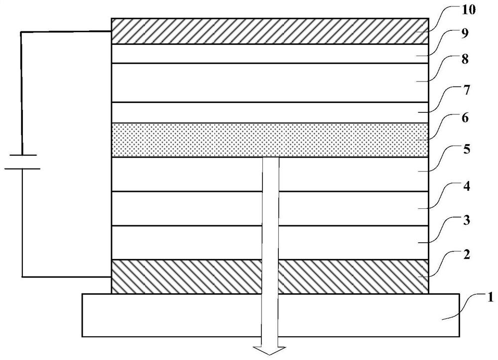
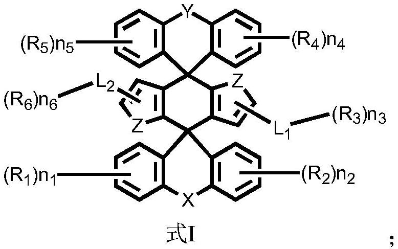
The invention provides a compound and an organic light-emitting device, a display panel and a display device comprising the compound. The compound has the structure shown in formula I. The organic light-emitting device includes an anode, a cathode, and an organic thin film layer between the anode and the cathode, and the organic thin film layer includes a light-emitting layer, and also includes one of a hole transport layer, an electron blocking layer, and a light-emitting auxiliary layer. one or a combination of at least two; at least one of the hole transport layer, the electron blocking layer and the luminescence assisting layer contains at least one of the compounds. The compound provided by the invention has shallower HOMO energy level, shallower LUMO energy level and higher triplet state energy level, suitable hole mobility, higher T g , large molecular torque, not easy to crystallize, good thermal stability, can be used in the hole transport layer, electron blocking layer and / or luminescence auxiliary layer of organic light-emitting devices, reduce the operating voltage of the device, improve the luminous efficiency and life of the device.

Description

technical field [0001] The invention belongs to the technical field of organic photoelectric materials, and in particular relates to a compound and an organic light-emitting device, a display panel and a display device containing the same. Background technique [0002] Organic light-emitting device (OLED device) is a light-emitting device based on organic light-emitting materials, which has attracted wide attention due to its many advantages such as high-efficiency light emission, simple manufacturing process, and large-area flexibility. At present, OLED devices have basically met the requirements of small and medium-sized displays, and are widely used in flat panel display and lighting fields such as instrumentation, high-end smartphones, and televisions. [0003] In addition to the necessary light-emitting layer, an OLED device usually contains one or more functional layers in a hole injection layer, a hole transport layer, an electron blocking layer, a hole blocking layer...

Claims


Application Information

Patent Timeline
Patent Type & Authority Patents(China)
IPC IPC(8): C07D491/22C07D493/10C07D493/22C07D495/10C07D495/22C07D519/00C07F7/08H01L51/54
CPCC07D495/22C07D519/00C07D491/22C07D493/22C07D495/10C07F7/0816C07D493/10H10K85/636H10K85/631H10K85/6576H10K85/6574H10K85/6572H10K85/657H10K85/40C09K11/06H10K85/653H10K85/655H10K85/615H10K50/156C09K2211/1018H10K85/626H10K50/11H10K50/15H10K50/16H10K50/17H10K50/18H10K50/171
Inventor 冉佺高威牛晶华张磊代文朋
Owner WUHAN TIANMA MICRO ELECTRONICS CO LTD
Learn More