

Compounds, organic light-emitting device comprising same, display panel and display device
An organic light-emitting device and compound technology, applied in the field of organic optoelectronic materials, can solve the problems of low triplet energy level, adjacent pixel crosstalk, slow material mobility, etc., to improve the luminous efficiency and lifespan, reduce the working voltage, and molecular torque. big effect
- Summary
- Abstract
- Description
- Claims
- Application Information
AI Technical Summary
Problems solved by technology
Method used
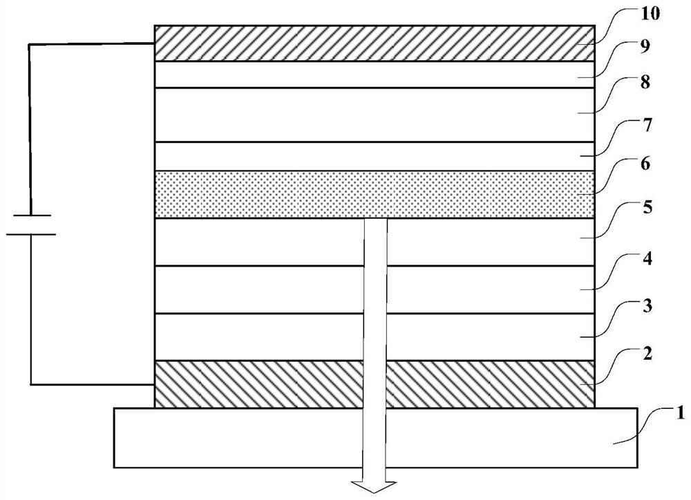
Image


Examples
preparation example 1
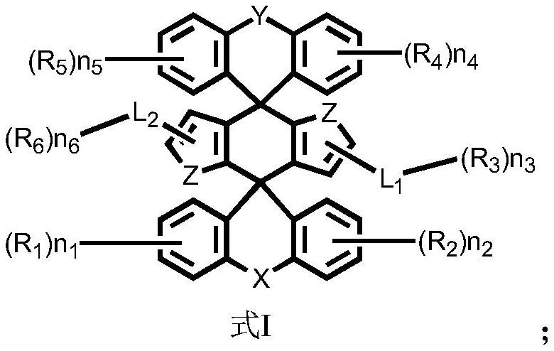
[0100] This preparation example provides compound 134 The specific preparation method is as follows:
[0101] (1)
[0102] Under nitrogen atmosphere, in 200mL of anhydrous toluene (Tol), add raw materials in sequence: Compound A (5mmol), diphenylamine (11mmol), sodium tert-butoxide (t-BuONa) (12.5mmol), tris(dibenzylideneacetone ) Dipalladium (Pd 2 (dba)3) (0.25mmol), and 2-dicyclohexylphosphine-2',6'-dimethoxybiphenyl (S-Phos) (0.75mmol), deoxygenated for 10min, heated to 110°C, reacted 24h. After the reaction is completed, cool and filter with suction, collect the filtrate, add water and dichloromethane for extraction and separation, collect the organic phase and dry it with anhydrous sodium sulfate, collect the filtrate with suction, spin off the solvent, and purify by column chromatography to obtain the intermediate B (78% yield).
[0103] LC-MS: m / z: Calculated: C34H22N2O2S2: 554.68, Found: 554.31.
[0104] (2)
[0105] Under nitrogen atmosphere, add reactant ...
preparation example 2
[0110] This preparation example provides compound 14 The specific preparation method is as follows:
[0111]
[0112] The difference between the preparation method of this organic compound 14 and Example 1 is that the 2-bromodiphenyl ether in the step (2) of Example 1 is With an equimolar amount of 2-bromotriphenylamine Instead, other raw materials, reaction steps and reaction conditions were the same as in Example 1, and finally the target product 2 was obtained (yield 62%).
[0113] LC-MS: m / z: Calculated: C70H48N4S2: 1009.29, Found: 1008.81.
[0114] Compound elemental analysis results: calculated value: C70H48N4S2 (%): C 83.30, H 4.79, N 5.55; test value: C 83.29, H 4.78, N 5.57.
preparation example 3
[0116] This preparation example provides compound 302 The specific preparation method is as follows:
[0117]
[0118] The difference between the preparation method of this organic compound 302 and Preparation Example 1 is that the 2-bromodiphenyl ether in the step (2) of Preparation Example 1 With an equimolar amount of 1-bromo-2-(1-methyl-1-phenyl-ethyl)-benzene Instead, other raw materials, reaction steps and reaction conditions were the same as those in Preparation Example 1, and finally the target product 3 was obtained (yield 60%).
[0119] LC-MS: m / z: Calculated: C64H50N2S2: 911.23, Found: 910.89.
[0120] Compound elemental analysis results: calculated value: C64H50N2S2 (%): C 84.36, H 5.53, N 3.07; test value: C 84.37, H 5.55, N 3.06.
PUM
| Property | Measurement | Unit |
|---|---|---|
| thickness | aaaaa | aaaaa |
| thickness | aaaaa | aaaaa |
| current efficiency | aaaaa | aaaaa |
Abstract
Description
Claims
Application Information