A kind of hemispherical microlens and preparation method thereof

A microlens and hemispherical technology, applied in the fields of optics and electronics, can solve the problems of large half-width of the focused beam beam, low light intensity, short working distance of the microsphere lens, etc., and achieve the goal of reducing the half-width and having a large market prospect Effect

Active Publication Date: 2021-08-17
UNIV OF ELECTRONICS SCI & TECH OF CHINA
View PDF5 Cites 0 Cited by
  • Summary
  • Abstract
  • Description
  • Claims
  • Application Information

AI Technical Summary

Problems solved by technology

[0004] The technical problem mainly solved by the present invention is to provide a microsphere lens, which can solve the problems in the prior art that the working distance of the microsphere lens is relatively short, the beam waist half-width of the focused beam is relatively large, and the light intensity is low. A microlens with longer working distance, narrower subwavelength beam waist FWHM, and higher light intensity, which can be applied to optical far-field subwavelength imaging or lithography, and can also be used for parallel imaging or parallel lithography

Method used


Image

  • A kind of hemispherical microlens and preparation method thereof
  • A kind of hemispherical microlens and preparation method thereof
  • A kind of hemispherical microlens and preparation method thereof

Examples


Embodiment 1

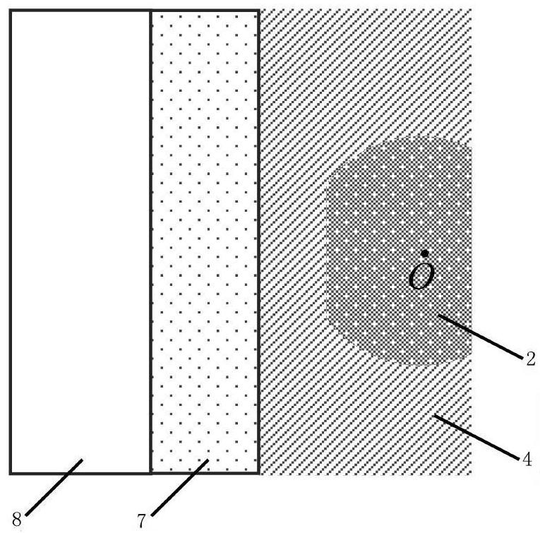
[0034] Such as figure 2 Shown, a kind of hemispherical microlens comprises at least one lens body 2, and described lens body 2 is: selected standard microsphere lens 2 ' a surface passing through the center of the sphere, on the surface passing through the center of the sphere Part of the spherical surface is cut off in parallel on both sides.

[0035] Further, it also includes a second material film layer 4, the lens body 2 is soaked in the second material film layer 4, a cut surface of the lens body 2 is located on the surface of the second material film layer 4, and the second material can also be made The surface of the film layer (4) is higher than the cut plane of the lens body (2).

[0036] The working principle of the hemispherical microlens in the present invention is: its part of the spherical surface is cut and removed by a plane parallel to the plane of the hemispherical microlens, and then soaked in the material film layer, when the incident light parallel to th...

Embodiment 2

[0042] In this embodiment, a kind of preparation method of the soaked hemispherical microlens is provided, such as figure 1 As shown, the method includes the following steps:

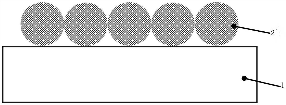
[0043] S1. If image 3 , 4 As shown, the self-assembled flat standard microsphere lens 2' is self-assembled on the first substrate 1, and the first material film layer 3 and the second material film layer 3 are sequentially grown on the obtained first substrate 1 on the side close to the microsphere lens 2'. Material film layer 4;

[0044] S2. If Figure 5 , 6 As shown, remove the first material film layer 3' and the second material film layer 4' covering the top of the microsphere lens 2', and then remove the remaining second material film 4" higher than the microsphere lens 2' The plane part of , get the first sample;

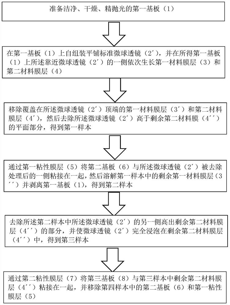
[0045] S3. If Figure 7 , 8 As shown, through the first adhesive film layer 5, the second substrate 6 and the side of the microsphere lens 2′ after the removal process are bond...

Embodiment 3

[0056] In an exemplary embodiment, a method of preparing a soaked hemispherical microlens comprises the steps of:

[0057] (1) Prepare a clean, dry, double-sided precision polished quartz plate, the size is: 15mm*15mm.

[0058] (2) A certain polished surface of the quartz plate prepared in (1) is tiled to obtain a single-layer microsphere lens array through the gas-liquid interface self-assembly method. The rate is 1.55.

[0059] (3) Copper and magnesium fluoride are vertically grown on one side of the quartz plate in (2) by the electron beam evaporation coating method, the growth rate is about 0.5nm / s, the thickness of the copper film is 2000nm, and the thickness of magnesium fluoride is 2500nm, the total thickness is 4500nm.

[0060] (4) Combining ultrasonic cleaning and mechanical peeling (blue film tape peeling) to remove the magnesium fluoride above the sample microspheres obtained in (3).

[0061] (5) Put the sample piece obtained in (4) into an oven horizontally, set...


PUM

PropertyMeasurementUnit
diameteraaaaaaaaaa
refractive indexaaaaaaaaaa

Abstract

The invention discloses a hemispherical microlens and a preparation method thereof. The lens includes at least one lens body (2), and the lens body (2) is: a standard microsphere lens (2') passing through a ball The surface of the center, and part of the spherical surface is cut in parallel on both sides of the surface passing through the center of the sphere. The preparation method is to cut off part of the spherical surface in parallel on both sides of the standard microsphere lens, and then soak it in the second material film layer (4). When the incident light parallel to the optical axis is incident on the partially cut spherical surface of the hemispherical microlens When , the light passing through the cut spherical surface will not participate in the formation of the spot, which is beneficial to improve the half-width of the spot; the light passing through the uncut spherical surface is farther away from the optical axis, forming a focal spot with a longer working distance, It can be applied in far-field parallel imaging / lithography to improve the efficiency of pattern parallel imaging / lithography with feature sizes close to or greater than 300nm.

Description

technical field [0001] The invention relates to the technical fields of optics and electronics, in particular to a hemispherical microlens and a preparation method thereof. Background technique [0002] As the integration of semiconductor devices increases, the size of components on semiconductor devices tends to be on the order of micronano, and imaging systems or photolithography systems with 200nm-400nm resolution are required in more scenarios. Due to the limitation of the optical diffraction limit of traditional optical lenses, coupled with the influence of light source quality and system optical path, it is difficult for metallographic microscopes to see particles with a size of 300nm. In addition, the size of traditional lenses is large, and it is difficult to make a lens array to achieve parallel work to improve work efficiency. Other high-resolution imaging systems, such as atomic force microscopes and scanning electron microscopes, not only have high equipment cos...

Claims


Application Information

Patent Timeline
Patent Type & Authority Patents(China)
IPC IPC(8): G02B3/00
CPCG02B3/0025G02B3/0037
Inventor 刘贤超王军苟君周泓希韩琦
Owner UNIV OF ELECTRONICS SCI & TECH OF CHINA
Why Eureka
Try Eureka