GaN-based vertical structure micro-cavity Micro-LED based on electroplating technology and preparation method thereof

A vertical structure and technology technology, applied in the direction of circuits, electrical components, semiconductor devices, etc., can solve the problems of limited bandwidth and slow luminous rate, and achieve the effect of improving brightness, fast luminous speed, and improving the directionality of front light emission

Pending Publication Date: 2020-09-29
长沙安牧泉智能科技有限公司
View PDF0 Cites 2 Cited by
  • Summary
  • Abstract
  • Description
  • Claims
  • Application Information

AI Technical Summary

Problems solved by technology

However, GaN-based Micro-LEDs have a very slow luminous rate due to the piezoelectric polarization effect of their MQW (quantum well), which greatly limits the bandwidth of Micro-LEDs as light sources for visible light communication.

Method used


Image

  • GaN-based vertical structure micro-cavity Micro-LED based on electroplating technology and preparation method thereof
  • GaN-based vertical structure micro-cavity Micro-LED based on electroplating technology and preparation method thereof
  • GaN-based vertical structure micro-cavity Micro-LED based on electroplating technology and preparation method thereof

Examples


Embodiment 1

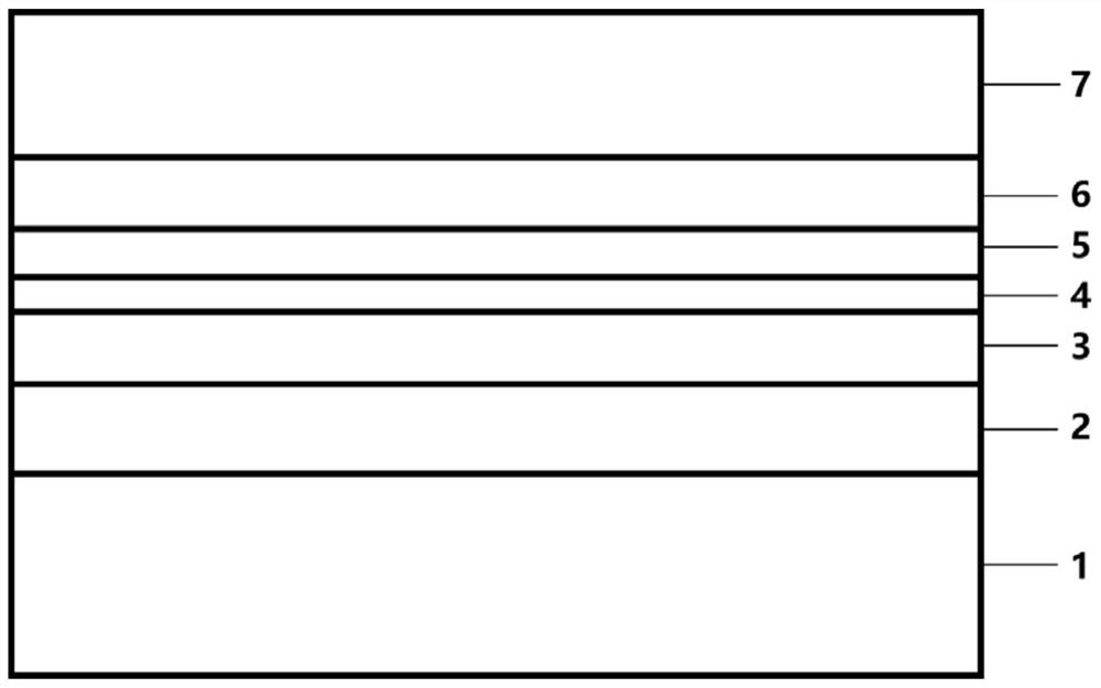
[0045] The structure of the vertical microcavity GaN-based Micro-LED of the present invention is as follows: Figure 9 As shown, it includes a Micro-LED chip and a substrate 7, and the Micro-LED chip is located on the substrate 7; the Micro-LED chip includes a dielectric film 10, an n-GaN layer 3, an MQW layer 4, a p -GaN layer 5 and reflector electrode 6, wherein reflector electrode 6 and substrate seven 7 join; The width of the bottom seven 7 is equal; the width of the dielectric film 10 is smaller than the n-GaN layer 3, and the mesa 11 will leak out on both sides of the n-GaN layer; the width of the mirror electrode is larger than the n-GaN layer 3, MQW layer 4, p -GaN layer 5, the mesa 11 will leak out on both sides of the mirror electrode 6, and the n-GaN layer 3, the MQW layer 4, and the p-GaN layer 5 will leak out two sidewalls; there is a passivation layer on the mesa 11 and the sidewall 8; The shape of the passivation layer 8 is a right-angled Z-shape; the passivati...

Embodiment 2

[0048] The preparation method of the vertical microcavity GaN-based Micro-LED provided in this embodiment includes the following steps:

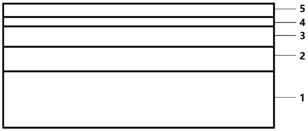
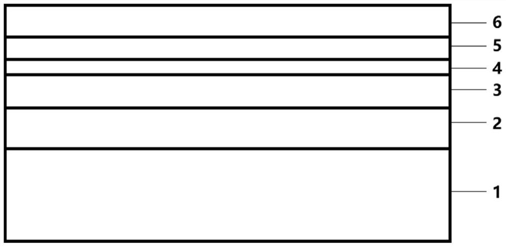
[0049] (1) On the (0001) plane sapphire (substrate 1), grow u-GaN layer 2 (5 μm in thickness), n-GaN layer 3 (5 μm in thickness), [InGaN (2nm) / GaN (10nm)] 8 MQW (quantum well) layer 4 (thickness is 96nm), p-GaN layer 5 (thickness is 100nm), obtains LED epitaxy material, and its luminescence wavelength is determined by the In composition in MQW (quantum well) layer 4, in this implementation In the example, the emission wavelength is 460nm. The structure of the obtained LED epitaxial material in step (1) is as follows: figure 1 shown.

[0050] (2) make reflector electrode 6 in p-GaN layer 5 by electron beam evaporation method, wherein, deposition temperature is 120 ℃, reflector electrode is Ni / Ag / Pt / Au, and the thickness of reflector electrode 6 is 0.5 / 200 / 50 / 200nm. The structure obtained after this step is as follows figure 2 shown. ...

Embodiment 3

[0060] The preparation method of the vertical microcavity GaN-based Micro-LED provided in this embodiment includes the following steps:

[0061] (1) First, grow u-GaN layer 2 (5 μm in thickness), n-GaN layer 3 (5 μm in thickness), [InGaN (2 nm) / GaN ( 10nm)] 8 MQW (quantum well) layer 4 (thickness: 96nm), p-GaN layer 5 (thickness: 100nm), to obtain LED epitaxial material. The structure of the obtained LED epitaxial material in step (1) is as follows figure 1 shown.

[0062] (2) The mirror electrode 6 is fabricated on the p-GaN layer 5 by electron beam evaporation, wherein the deposition temperature is 120 degrees, and the mirror electrode is Ni / Ag / Pt / Au. The thickness of the mirror electrode 6 is 0.5 / 200 / 50 / 200 nm. The structure obtained after this step is as follows figure 2 shown.

[0063] (3) Prepare a substrate 7 on the reflector electrode 6 obtained in step (2) by electroplating. Specifically, a layer of Cu is electroplated with a copper-plating electroplating solu...


PUM

PropertyMeasurementUnit
sizeaaaaaaaaaa
thicknessaaaaaaaaaa
thicknessaaaaaaaaaa

Abstract

The invention discloses a GaN-based vertical structure micro-cavity Micro-LED based on an electroplating technology and a preparation method thereof. The micro-cavity Micro-LED is narrow in light-emitting full width at half maximum and good in light-emitting directivity; thickness of a chip is reduced, and a metal reflector of the p-GaN layer (5) and a dielectric film reflector of the n-GaN layerare used as end faces of a resonant cavity to form a resonant micro-cavity structure in the vertical direction, so side wall light emission is inhibited, front light emission directivity is improved,and the crosstalk effect between adjacent pixels of Micro-LED display is reduced. Meanwhile, the resonant micro-cavity structure selects a specific wavelength, so the light-emitting spectrum is narrowed, the spectral purity is higher, the display threshold of the Micro-LED is improved, a Micro-LED active region of the vertical structure is large in area, and n-GaN light absorption is less, the current expansion is good, the voltage is low, the current density is small, and advantages in the aspects of lighting effect, saturation current and long-term reliability are achieved; and secondly, a Cu substrate has good electrical conductivity and thermal conductivity, and thermal resistance of the chip is small.

Description

technical field [0001] The invention relates to the field of semiconductor technology, in particular to a GaN-based vertical structure microcavity Micro-LED based on electroplating technology and a preparation method thereof. Background technique [0002] Micro-LED has important applications in display and visible light communication. The display industry is a leading industry in the information age, with an annual output value of more than 100 billion U.S. dollars. Light-emitting diodes (LEDs) have gradually become the mainstream in the field of display lighting due to their irreplaceable advantages of energy saving, high efficiency, durability, and mercury-free. Due to its excellent characteristics such as ultra-high resolution, high brightness, ultra-power saving and fast response, Micro-LED is considered to be the most potential display technology after TFT-LCD and AMOLED technology. In Micro-LED display, the size of pixel unit is reduced to improve display accuracy and...

Claims


Application Information

Patent Timeline
Patent Type & Authority Applications(China)
IPC IPC(8): H01L33/10H01L33/06H01L33/32H01L33/00
CPCH01L33/007H01L33/06H01L33/10H01L33/105H01L33/32
Inventor 汪炼成高祥万荣桥徐意
Owner 长沙安牧泉智能科技有限公司
Why Eureka
Try Eureka