MicroLED preparation method based on three-dimensional mask substrate

A mask and three-dimensional technology, which is applied in semiconductor devices, electrical components, circuits, etc., can solve the problems of time-consuming, small size of Micro LED, and shift of light emission wavelength, and achieve the goals of solving wavelength drift, improving detection efficiency, and low defect density Effect

Active Publication Date: 2020-10-16
北京飓芯科技有限公司
View PDF5 Cites 0 Cited by
  • Summary
  • Abstract
  • Description
  • Claims
  • Application Information

AI Technical Summary

Problems solved by technology

Because of the small size of the MicroLED, it is intolerable for the local high dislocation density area, because the local high dislocation density will cause the device to be inconsistent with other devices, or even fail completely.
From this point of view, although the high quality of the wing area of ​​ELOG technology can meet the crystal quality requirements of Micro LED, the high dislocation density in the window area is unacceptable.
[0007] 4) In terms of production cost, Micro LED also has strict restrictions
Mass production of Micro LEDs using homogenous substrates is unrealistic because the price is too high for the market to accept
On the other hand, the use of laser lift-

Method used


Image

  • MicroLED preparation method based on three-dimensional mask substrate
  • MicroLED preparation method based on three-dimensional mask substrate
  • MicroLED preparation method based on three-dimensional mask substrate

Examples


Example Embodiment

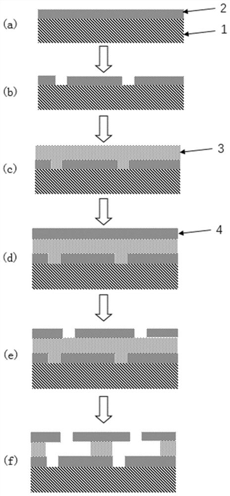
[0046] In order to make the above objectives, features and advantages of the present invention more obvious and easy to understand, the present invention will be further described in detail below through specific embodiments and drawings, taking GaN in group III nitride materials as an example.

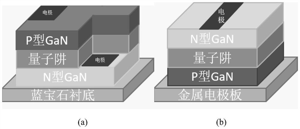
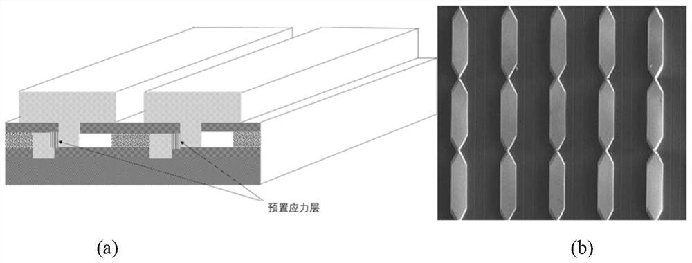
[0047] In the present invention, the three-dimensional mask substrate technology used can firstly provide ultra-high crystal quality GaN material for the epitaxial device structure of MicroLED, thereby solving the demand for high crystal quality in MicroLED, and overcoming many problems due to insufficient crystal quality. The problem caused. The second aspect is the easy peeling characteristics of the three-dimensional mask technology, and the stripped monomer has small bumps, which facilitates the adsorption and grabbing of the MicroLED during the mass transfer process, which can well meet the needs of the MicroLED for easy peeling and easy transfer . In the third aspect, the size can...


PUM

PropertyMeasurementUnit
Thicknessaaaaaaaaaa

Abstract

The invention relates to a MicroLED preparation method based on a three-dimensional mask substrate. The method comprises the following steps: preparing a three-dimensional mask layer on a heterogeneous substrate; epitaxially growing a group III nitride material on the heterogeneous substrate by using the three-dimensional mask layer; and carrying out epitaxial growth of a MicroLED structure layeron the III-group nitride material. According to the method, a preset stress layer is inserted in a channel growth stage in a growth process on a three-dimensional mask substrate aiming at the characteristics of the three-dimensional mask substrate and higher crystal quality requirements of a MicroLED; in the electrode manufacturing process, SiNx is used for replacing common SiO2 to serve as an insulating protection layer; the substrate is stripped by using a wet etching method; and a KOH solution is adopted to treat the bottom of the MicroLED so as to improve the light extraction efficiency.

Description

technical field [0001] The invention belongs to the technical field of micro light-emitting diode displays, and in particular relates to a preparation method of Micro LED based on a three-dimensional mask substrate. Background technique [0002] Micro LED Display (Micro LED Display) is a new generation of display technology. The structure is a miniaturized LED array, that is, the LED structure design is thinned, miniaturized and arrayed, so that its volume is about 1 times the size of the current mainstream LED. %, reaching a size range of 10-30um, each pixel can be addressed and driven to emit light independently, and the distance between pixels is reduced from the original millimeter level to the micron level. Inheriting the characteristics of LED, the advantages of Micro LED include low power consumption, high brightness, ultra-high resolution and color saturation, fast response, super power saving, long life, high efficiency, etc., and its power consumption is about LCD ...

Claims


Application Information

Patent Timeline
IPC IPC(8): H01L33/00
CPCH01L33/007
Inventor 张晓蓉郑烨琳冯筱陈明兰
Owner 北京飓芯科技有限公司
Why Eureka
Try Eureka