Silicon-based gallium nitride microwave millimeter wave transmission line with low electromagnetic loss and preparation method thereof

A silicon-based nitrogen, low-electromagnetic technology, applied in circuits, waveguides, electrical components, etc., can solve the problems of high electromagnetic loss, high background carrier concentration of microwave and millimeter-wave transmission lines, and limiting the performance of gallium nitride on silicon transmission lines, etc.

Active Publication Date: 2020-10-27
XIDIAN UNIV
View PDF3 Cites 0 Cited by
  • Summary
  • Abstract
  • Description
  • Claims
  • Application Information

AI Technical Summary

Problems solved by technology

The high defect density in the AlN nucleation layer also results in a high background carrier concentration
These factors make GaN-on-Si micr

Method used


Image

  • Silicon-based gallium nitride microwave millimeter wave transmission line with low electromagnetic loss and preparation method thereof
  • Silicon-based gallium nitride microwave millimeter wave transmission line with low electromagnetic loss and preparation method thereof
  • Silicon-based gallium nitride microwave millimeter wave transmission line with low electromagnetic loss and preparation method thereof

Examples


Embodiment 1

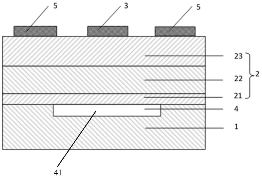
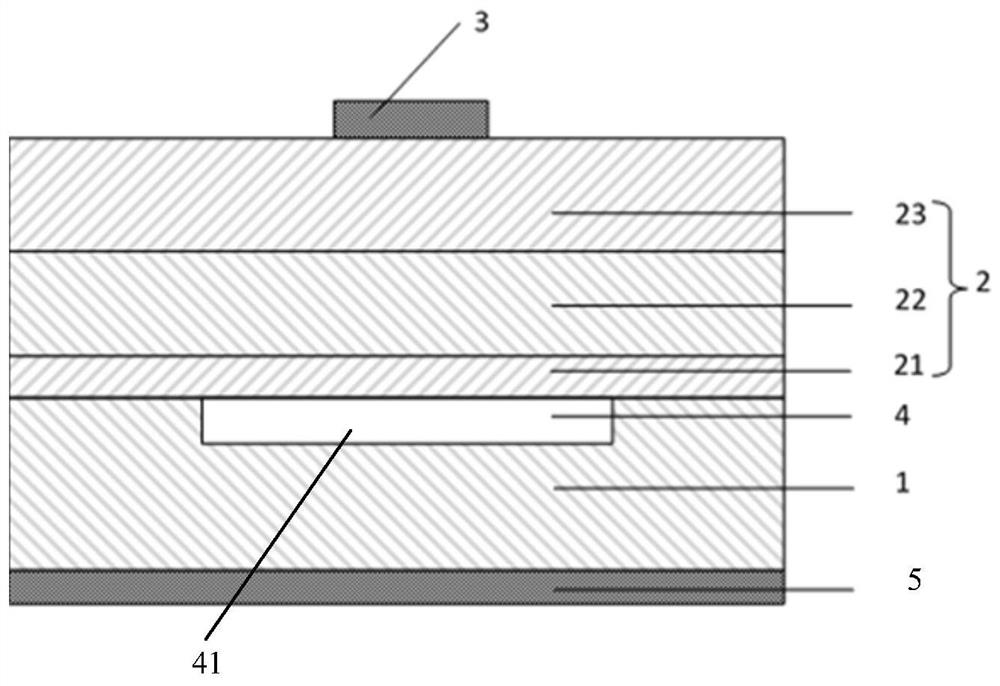
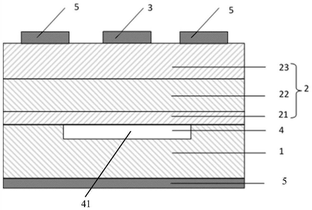
[0051] When Group III nitride materials including gallium nitride are epitaxially grown on a silicon substrate, aluminum atoms and gallium atoms will diffuse into the silicon substrate to form a p-type doped parasitic conductive channel. In addition, due to the existence of polarized charges in the III-nitride, an n-type inversion conduction channel exists at the silicon / nitride interface. These factors make the GaN-on-Si microwave and millimeter wave transmission line have high electromagnetic loss, which reduces the performance of the transmission line. At present, the main measures to suppress the electromagnetic loss of silicon-based GaN microwave and millimeter wave transmission lines are: 1. Optimize the thickness and growth conditions of the aluminum nitride nucleation layer, using a relatively thin aluminum nitride nucleation layer, but using a relatively thin The aluminum nitride nucleation layer will affect the quality of the subsequent transition layer of the III-ni...

Embodiment 2

[0076] When Group III nitride materials including gallium nitride are epitaxially grown on a silicon substrate, except for the p-type doped channel on the surface of the silicon substrate and the silicon / aluminum nitride interface described in Embodiment 1 In addition to the influence of the n-type inversion channel on the electromagnetic loss of GaN-on-Si transmission line, the dislocation and defect density of the nucleation layer and the transition layer are relatively high, and the background impurity concentration is also relatively high, which will also bring a certain degree of Electromagnetic loss. The current main measures to suppress the electromagnetic loss of GaN-on-Si microwave and millimeter wave transmission lines described in Embodiment 1 have little effect on eliminating the electromagnetic loss of the nucleation layer and buffer layer, and also have the same effect as described in Embodiment 1. Shortcomings. Based on the above-mentioned problems, in order to...

Embodiment 3

[0101] On the basis of the above embodiments, this embodiment provides a method for manufacturing a GaN-on-Si microwave and millimeter wave transmission line with low electromagnetic loss.

[0102] Described preparation method comprises:

[0103] S1: Select a silicon substrate;

[0104] S2: preparing a III-nitride epitaxial layer on the upper surface of the silicon substrate;

[0105] S3: Etching an internal cavity on the contact surface between the silicon substrate and the III-nitride epitaxial layer;

[0106] S4: preparing a high-frequency signal metal electrode on the upper surface of the III-nitride epitaxial layer;

[0107] S5: Prepare ground metal electrodes on both sides of the high-frequency signal metal electrodes and / or on the lower surface of the silicon substrate.

[0108] Further, said S2 includes:

[0109] S21: Prepare a nucleation layer with a thickness of 50nm-500nm on the upper surface of the silicon substrate by MOCVD equipment;

[0110] S22: Using MOCV...


PUM

PropertyMeasurementUnit
Heightaaaaaaaaaa
Thicknessaaaaaaaaaa
Thicknessaaaaaaaaaa

Abstract

The invention discloses a silicon-based gallium nitride microwave millimeter wave transmission line with low electromagnetic loss and a preparation method thereof. The silicon-based gallium nitride microwave millimeter wave transmission line comprises a silicon substrate, a III-nitride epitaxial layer, a high-frequency signal metal electrode and grounding metal electrodes, wherein the III-nitrideepitaxial layer is arranged on the upper surface of the silicon substrate; the high-frequency signal metal electrode is arranged on the upper surface of the III-nitride epitaxial layer; the groundingmetal electrodes are arranged on the two sides of the high-frequency signal metal electrode and/or the lower surface of the silicon substrate, an internal cavity is formed between the silicon substrate and the III-nitride epitaxial layer, and at least one part of the internal cavity is formed in the silicon substrate. The silicon-based gallium nitride microwave millimeter wave transmission line can effectively reduce the electromagnetic loss of a silicon-based gallium nitride material, improves the output power and efficiency of a silicon-based gallium nitride microwave millimeter wave device,and meets the application requirements of a microwave millimeter wave radio frequency circuit and system.

Description

technical field [0001] The invention belongs to the technical field of semiconductor devices, and in particular relates to a silicon-based gallium nitride microwave and millimeter wave transmission line with low electromagnetic loss and a preparation method thereof. Background technique [0002] The third-generation semiconductor material gallium nitride has the advantages of wide band gap, high critical breakdown field strength, high electron mobility, and high saturation electron drift velocity. It has great development potential in the field of microwave and millimeter wave high-power electronic devices, and can be widely used It is used in aerospace, radar, 5G communication and other fields. There are two types of gallium nitride epitaxy: homoepitaxy and heterogeneous epitaxy. Since the cost of gallium nitride homogeneous epitaxy is very high, the commonly used technology is heterogeneous epitaxy. The commonly used substrates for mainstream gallium nitride heteroepitaxy...

Claims


Application Information

Patent Timeline
IPC IPC(8): H01L23/66H01P3/00H01P11/00
CPCH01L23/66H01P3/003H01P11/001H01L2223/6627
Inventor 刘志宏宋昆璐张进成刘俊伟郝璐周弘赵胜雷张苇杭段小玲郝跃
Owner XIDIAN UNIV
Why Eureka
Try Eureka