
Resistive random access memory structure and manufacturing method thereof

A technology of resistive random access memory, applied in the direction of electric solid devices, circuits, electrical components, etc., can solve the process complexity, increase in production cost and production time, and reduce the reliability and yield of resistive random access memory , memory cell damage, etc., to increase the complexity, improve yield and reliability, and improve mechanical strength.

Pending Publication Date: 2020-10-27
WINBOND ELECTRONICS CORP
View PDF5 Cites 0 Cited by
  • Summary
  • Abstract
  • Description
  • Claims
  • Application Information

AI Technical Summary

Problems solved by technology

If the above-mentioned openings in the array area and the peripheral area are formed under the same conditions, the memory cells may be damaged due to excessive corrosion, thereby reducing the reliability and yield of the RRAM
On the other hand, if the above-mentioned openings in the array region and the peripheral region are formed in different etching steps, the complexity of the process, production cost and production time will be greatly increased.

Method used


Image

  • Resistive random access memory structure and manufacturing method thereof
  • Resistive random access memory structure and manufacturing method thereof
  • Resistive random access memory structure and manufacturing method thereof

Examples


Embodiment Construction

[0036] In order to make the purpose, features and advantages of the present invention more comprehensible, preferred embodiments are listed below and described in detail in conjunction with the accompanying drawings.

[0037] Herein, the dielectric constant of the low-k dielectric material is less than 3. Materials for low-k dielectric layers can include SiLK TM , low dielectric constant flowable oxide (low k-flowable oxide, FOx), fluorinated silicate glass (Fluorinated silicate glass, FSG), hydrogen silsesquioxane (hydrogen silsesquioxane, HSQ), methyl silicon times Methylsilsesquioxane (MSQ), Nanoglass, Black Diamond TM 、Coral TM 、Aurora TM or other known low-k dielectric materials.

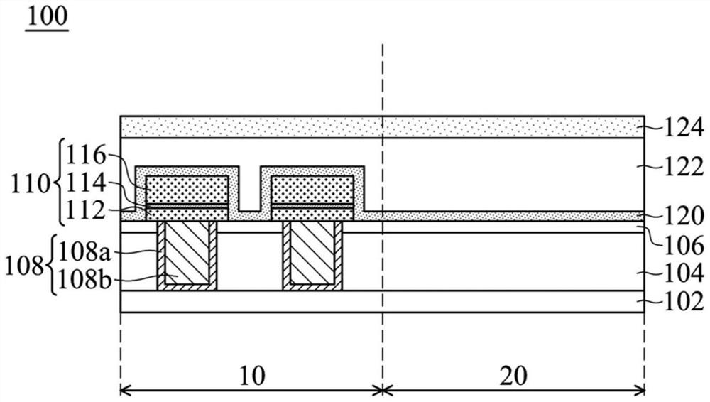
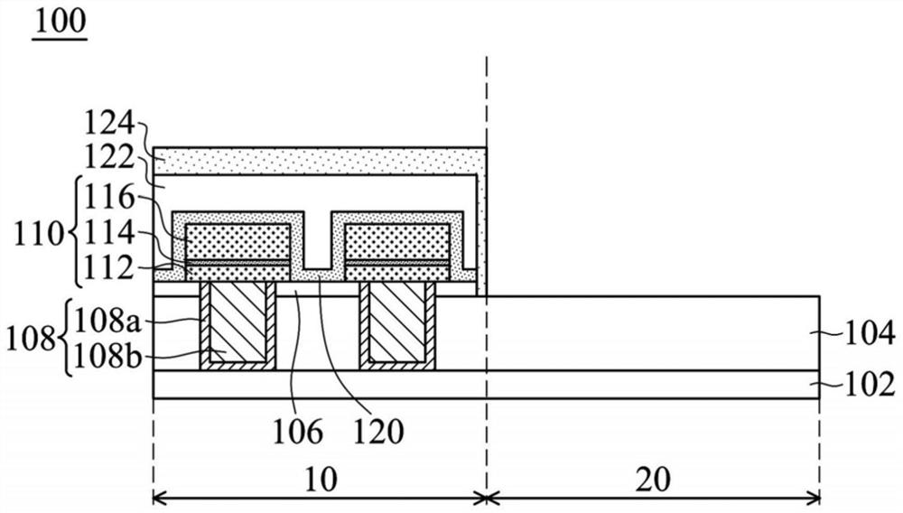
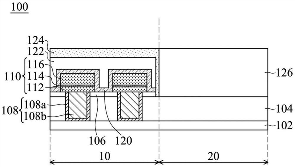
[0038] Figure 1A to Figure 1G It is a cross-sectional diagram corresponding to each step of the manufacturing method of the RRAM structure 100 according to some embodiments of the present invention. Please refer to Figure 1A , the substrate 102 is provided, and the substrate 102 include...


PUM


Abstract

The invention provides a resistive random access memory structure and a manufacturing method thereof. The resistive random access memory structure includes a substrate, a plurality of memory cells, agap filling dielectric layer, a buffer layer, a first low dielectric constant dielectric layer and a first conductive plug, wherein the substrate is provided with an array region and a peripheral region; the plurality of memory cells and the gap filling dielectric layer covering the memory cells are located on the substrate and in the array region; the buffer layer is only located in the array region and covers the gap filling dielectric layer, and the material of the buffer layer is different from the material of the gap filling dielectric layer; the first low dielectric constant dielectric layer is only located in the peripheral region, and the material of the first low dielectric constant dielectric layer is different from the material of the buffer layer; a dielectric constant of the first low dielectric constant dielectric layer is less than 3; the top surface of the first low dielectric constant dielectric layer is coplanar with the top surface of the buffer layer; and the firstconductive plug penetrates through the buffer layer and the gap filling dielectric layer and is in contact with one of the memory cells.

Description

technical field [0001] The present invention relates to a memory device, and more particularly to a resistive random access memory structure and a manufacturing method thereof. Background technique [0002] Resistive random access memory (RRAM) has the advantages of simple structure, small area, low operating voltage, fast operating speed, long storage time, multi-state storage, and low power consumption. Therefore, the resistive random access memory has great potential to replace the current flash memory and become the mainstream of the next generation non-volatile memory. [0003] In known RRAMs, a chip usually includes an array area and a peripheral area. The array area includes a plurality of memory cells, and each memory cell includes a patterned bottom electrode layer, a resistive transition layer and a top electrode layer. The peripheral area is mainly logic circuits. In the peripheral area, in order to improve the operation speed of the logic circuit, the dielectr...

Claims


Application Information

Patent Timeline
Patent Type & Authority Applications(China)
IPC IPC(8): H01L27/24H01L45/00
CPCH10B63/80H10N70/011
Inventor 许博砚吴伯伦沈鼎瀛
Owner WINBOND ELECTRONICS CORP
Learn More