Triode control type hybrid structure full-color display device and manufacturing method thereof

A hybrid structure and display device technology, which is applied in semiconductor/solid-state device manufacturing, static indicators, electric solid-state devices, etc., can solve problems such as uneven coating of luminous media, unfavorable large-area production, and unfavorable high-integration system construction.

Active Publication Date: 2020-10-27
FUZHOU UNIV +1
View PDF7 Cites 3 Cited by
  • Summary
  • Abstract
  • Description
  • Claims
  • Application Information

AI Technical Summary

Problems solved by technology

For the RGB three-color chip method, it is still difficult to grow RGB three-color chips with different wavelengths on the same substrate, and the three colors must be driven separately, the driving circuit is complicated and the cost is high.
Other preparation methods also have problems such as full-color display deviation, low light conversion efficiency, uneven coating of luminescent medium, high preparation cost, harsh processing conditions, and unfavorable large-area production. Therefore, it is not conducive to the realization and development of high-quality commercial LED products. application
Chinese patent CN201810863787.2 discloses a full-color micro-LED device based on an inorganic/organic semiconductor hybrid structure and its preparation method. RGB three-color mo...

Method used


Image

  • Triode control type hybrid structure full-color display device and manufacturing method thereof
  • Triode control type hybrid structure full-color display device and manufacturing method thereof
  • Triode control type hybrid structure full-color display device and manufacturing method thereof

Examples


Embodiment 2

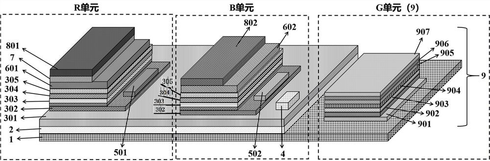
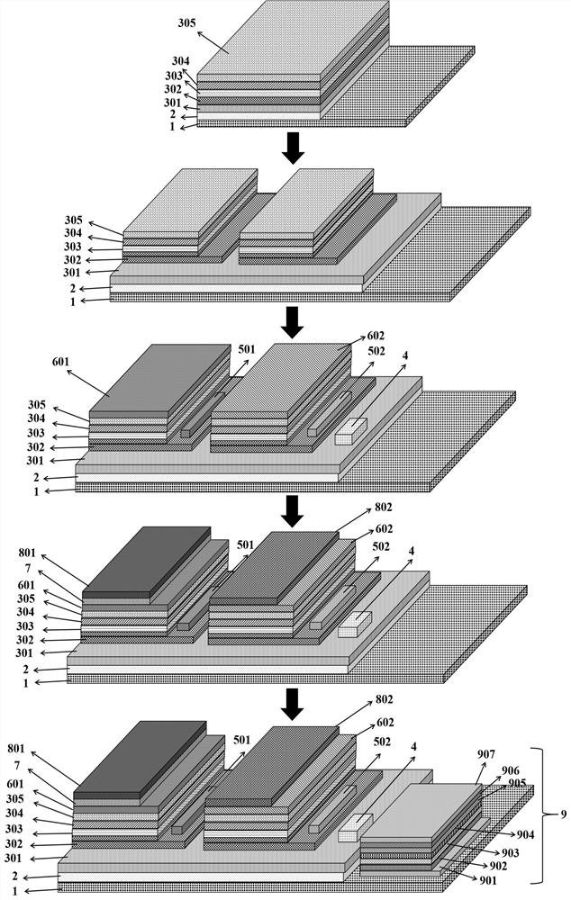
[0095] In this embodiment, the substrate 1 is a sapphire substrate, and is an a-plane, the material used for the buffer layer 2 is AlN, and the main material of the epitaxial layer is a GaN-based material. Specifically, the first layer on the buffer layer The semiconductor layer is an N-GaN layer, the second semiconductor layer on the buffer layer is a P-GaN layer, the third semiconductor layer on the buffer layer is an N-GaN layer, and the blue light emitting layer 304 is a three-period In a Ga 1-a N quantum well active layer and Al b Ga 1-b A hole blocking layer or an electron blocking layer composed of N, and the fourth semiconductor layer on the buffer layer is P-GaN. The first contact electrode 4 is a gold-copper electrode, the second contact electrode SCE1501 and the third contact electrode SCE2502 are gold-copper electrodes, and the transparent fourth contact electrode TCE1601 and fifth contact electrode TCE2602 are both indium tin oxide (ITO). The light conversion ...


PUM

PropertyMeasurementUnit
Thicknessaaaaaaaaaa
Thicknessaaaaaaaaaa
Thicknessaaaaaaaaaa

Abstract

The invention relates to a triode control type hybrid structure full-color display device and a manufacturing method thereof. According to the invention, a low-power variable input signal is respectively applied between a first contact electrode and a second contact electrode SCE1 and between the first contact electrode and a third contact electrode SCE2, a forward bias voltage is respectively applied between the first contact electrode and a fourth contact electrode TCE1 and between the first contact electrode and a fifth contact electrode TCE2; a blue light emitting chip in the unit B is driven to emit blue light, a blue light emitting chip in the unit R is driven to emit blue light so as to excite a red conversion layer to emit red light, a voltage is applied between a cathode and a transparent anode in the unit G, green light is excited, and thus full-color display is achieved. According to the invention, the first triode and the second triode amplify the power of an input signal,so that the light-emitting chip is driven to emit light by using a low-power input signal, the design complexity of a driving circuit of the light-emitting device can be effectively reduced, and the integration level of the display device is improved.

Description

technical field [0001] The invention relates to the design field of display semiconductor light-emitting devices, and relates to a triode-regulated hybrid structure full-color display device and a manufacturing method thereof. Background technique [0002] Light-emitting diodes (LEDs) are increasingly used in display applications due to their long life, small size, low power consumption, high brightness, and fast response. However, with the rapid development of information technology, traditional display technology can no longer meet the existing needs, and new micro-display technology with low power consumption, high brightness, wide color gamut, and ultra-high resolution has become more and more important. Micron-scale light-emitting diode (μLED) refers to the miniaturization of traditional LEDs to form a micron-scale pitch LED array to achieve ultra-high-density pixel resolution. It can be widely used in flexible, transparent displays, AR, VR and other fields. It is the m...

Claims


Application Information

Patent Timeline
IPC IPC(8): H01L27/32H01L27/15H01L33/06H01L33/10H01L33/50H01L51/50H01L51/56G09F9/33G09G3/32G09G3/3208
CPCH01L27/156H01L33/06H01L33/46H01L33/50G09F9/33G09G3/32G09G3/3208H10K59/35H10K50/115H10K50/11H10K71/00
Inventor 张永爱翁雅恋郭太良周雄图吴朝兴严群孙捷林志贤陈培崎
Owner FUZHOU UNIV
Why Eureka
Try Eureka