5G base station protection chip manufacturing process

A technology for protecting chips and manufacturing processes, which is applied in the field of 5G base station protection chip manufacturing processes, and can solve problems such as channel diffusion leakage current and poor chips

Inactive Publication Date: 2020-10-30
江苏晟驰微电子有限公司
View PDF7 Cites 5 Cited by
  • Summary
  • Abstract
  • Description
  • Claims
  • Application Information

AI Technical Summary

Problems solved by technology

[0005] Aiming at the deficiencies of the prior art, the present invention provides a 5G base station protection chip manufacturing process, which s...

Method used


Image

  • 5G base station protection chip manufacturing process
  • 5G base station protection chip manufacturing process

Examples


Embodiment Construction

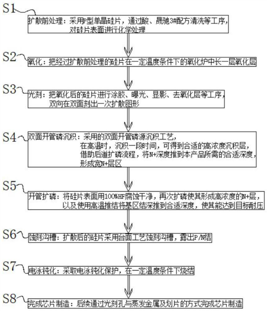
[0024] The following will clearly and completely describe the technical solutions in the embodiments of the present invention with reference to the accompanying drawings in the embodiments of the present invention. Obviously, the described embodiments are only some, not all, embodiments of the present invention.

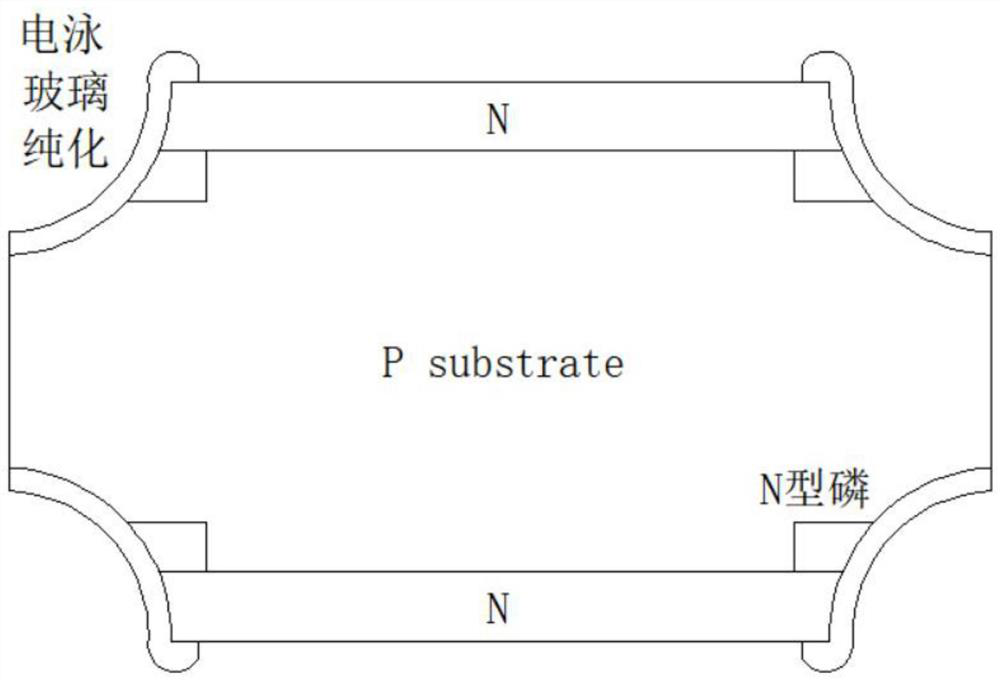
[0025] see Figure 1 to Figure 2 , the present invention provides a technical solution: a 5G base station protection chip manufacturing process, comprising the following steps:

[0026] S1. Pre-diffusion treatment: use P-type single crystal silicon wafers, and carry out chemical treatment on the surface of silicon wafers through processes such as cleaning with acid and Shengchi 3# formula;

[0027] S2. Oxidation: grow a layer of oxide layer on the silicon wafer that has been pre-diffused in an oxidation furnace at a certain temperature;

[0028] S3. Photolithography: apply glue, exposure, development, and deoxidation to the oxidized silicon wafer, and engrave a diff...


PUM


Abstract

The invention discloses a 5G base station protection chip manufacturing process and particularly relates to a 5G base station protection chip manufacturing process. The process comprises the followingsteps of S1, diffusion pretreatment; S2, oxidation; S4, double-sided tube opening phosphorus deposition; S5, opening a pipe and expanding phosphorus; S6, etching the groove; S7, electrophoresis passivation; and S8, completing chip manufacturing. A chip arranged in the 5G base station protection chip manufacturing process adopts a mesa process, an auxiliary groove structure is designed in an areanear the chip table board, when the highest reverse voltage is applied externally, the P-type base region depletion layer is limited in the base region, the breakdown voltage of the high-voltage transient voltage suppressor is higher than the breakdown voltage of the main body junction, so the main body junction region is broken down firstly, the leakage current is distributed in the main body junction region, the auxiliary junction region is not broken down, the voltage resistance of the high-voltage transient voltage suppressor is improved, and the surge resistance and reliability of the transient voltage suppressor are improved.

Description

technical field [0001] The invention relates to the technical field of 5G base stations, in particular to a 5G base station protection chip manufacturing process. Background technique [0002] 5G base station is the core equipment of 5G network, which provides wireless coverage and realizes wireless signal transmission between wired communication network and wireless terminal. The architecture and shape of base stations directly affect how 5G networks are deployed. In the technical standard, the frequency band of 5G is much higher than that of 2G, 3G and 4G networks. At this stage, the 5G network mainly works in the 3000-5000MHz frequency band. Since the higher the frequency, the greater the attenuation during signal propagation, so the base station density of the 5G network will be higher. [0003] Integrated circuits, or microcircuits, microchips, and chips are a way of miniaturizing circuits (mainly including semiconductor devices, but also passive components, etc.) in ...

Claims


Application Information

Patent Timeline
IPC IPC(8): H01L21/329H01L29/06H01L29/861
CPCH01L29/0611H01L29/0657H01L29/66121H01L29/8613
Inventor 崔文荣
Owner 江苏晟驰微电子有限公司
Why Eureka
Try Eureka