PCB secondary circuit gold plating process

A secondary circuit and process technology, applied in the field of PCB board manufacturing, can solve problems affecting product quality and cost, business competition success or failure, etc.

Inactive Publication Date: 2020-11-03
深圳市明正宏电子有限公司
View PDF5 Cites 0 Cited by
  • Summary
  • Abstract
  • Description
  • Claims
  • Application Information

AI Technical Summary

Problems solved by technology

The design and manufacturing quality of printed boards directly affect the quality and cos

Method used


Image

  • PCB secondary circuit gold plating process

Examples


Embodiment 1

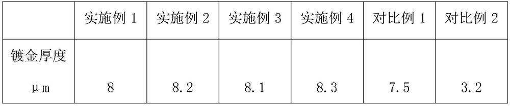
[0026] PCB secondary circuit gold plating process, including the following steps:

[0027] The first step is to grind and clean the PCB through a horizontal line to remove the oxide layer on the surface, and then print a layer of photosensitive solder resist ink on the surface of the PCB by screen printing, and then transfer it to a 65°C oven to dry the photosensitive solder resist ink. Bake for 2 hours, then put the PCB into an exposure machine for exposure for 20 seconds, then transfer it to a 1% sodium carbonate solution for cleaning, remove the unexposed photosensitive solder resist ink, and expose the gold-plated area pattern, and then send it to an oven at 135°C for drying 30min;

[0028] The second step is to pass the PCB through acid degreasing and micro-etching solution respectively to remove the oxide layer on the surface, and then open the skylight on the PCB surface corresponding to the position of the gold finger in the first gold-plated area on the PCB so that th...

Embodiment 2

[0037] PCB secondary circuit gold plating process, including the following steps:

[0038] The first step is to clean the PCB through a horizontal line to remove the oxide layer on the surface, and then print a layer of photosensitive solder resist ink on the surface of the PCB by screen printing, and then transfer it to a 65°C oven to dry the photosensitive solder resist ink. Bake for 2 hours, then send the PCB into an exposure machine for exposure for 20 seconds, then transfer it to a sodium carbonate solution with a mass fraction of 1% for cleaning, remove the unexposed photosensitive solder resist ink, and expose the pattern of the gold-plated area, and then send it to an oven at 135°C for drying 30min;

[0039] In the second step, the PCB is respectively subjected to acid degreasing and micro-etching solutions to remove the oxide layer on the surface, and then a skylight is opened on the PCB surface corresponding to the position of the gold finger in the first gold-plated...

Embodiment 3

[0048] PCB secondary circuit gold plating process, including the following steps:

[0049] The first step is to clean the PCB through a horizontal line to remove the oxide layer on the surface, and then print a layer of photosensitive solder resist ink on the surface of the PCB by screen printing, and then transfer it to a 65°C oven to dry the photosensitive solder resist ink. Bake for 2 hours, then send the PCB into an exposure machine for exposure for 20 seconds, then transfer it to a sodium carbonate solution with a mass fraction of 1% for cleaning, remove the unexposed photosensitive solder resist ink, and expose the pattern of the gold-plated area, and then send it to an oven at 135°C for drying 30min;

[0050] In the second step, the PCB is respectively subjected to acid degreasing and micro-etching solutions to remove the oxide layer on the surface, and then a skylight is opened on the PCB surface corresponding to the position of the gold finger in the first gold-plated...


PUM

PropertyMeasurementUnit
Thicknessaaaaaaaaaa

Abstract

The invention discloses a PCB secondary circuit gold plating process, which comprises the following steps of: grinding and cleaning a PCB through a horizontal line to remove an oxide layer on the surface of the PCB, printing a layer of photosensitive solder resist ink on the surface of the PCB in a silk screen skip printing manner, transferring the PCB into a 65 DEG C oven, baking the photosensitive solder resist ink for 2 hours, and feeding the PCB into an exposure machine for exposing for 20 seconds; then transferring into a sodium carbonate solution with the mass fraction of 1% for cleaning, removing the unexposed photosensitive solder resist ink to expose a gold plating area pattern, and then feeding into a oven at 135-140 DEG C for drying the PCB for 30 minutes. According to the invention, the conductive windows are formed during two times of gold plating, the positions of the conductive windows can be adjusted according to actual requirements, the reject ratio of gold staining ofthe conductive windows is reduced by forming the conductive windows, the gold salt cost is saved, and the purpose of thickening a gold layer can be achieved through two times of gold plating.

Description

technical field [0001] The invention belongs to the technical field of PCB board manufacturing, in particular to a PCB secondary circuit gold plating process. Background technique [0002] The Chinese name of PCB is printed circuit board, referred to as printed board, which is one of the important components of the electronics industry. Almost every kind of electronic equipment, ranging from electronic watches and calculators to computers, communication electronic equipment, and military weapon systems, as long as there are electronic components such as integrated circuits, printed boards are used for the electrical interconnection between them. . In the larger electronic product research process, the most basic success factors are the design, documentation and fabrication of the product's printed board. The design and manufacturing quality of printed boards directly affect the quality and cost of the entire product, and even lead to the success or failure of commercial co...

Claims


Application Information

Patent Timeline
IPC IPC(8): H05K3/24H05K3/28G03G9/08
CPCG03G9/081H05K3/241H05K3/282H05K2203/052
Inventor 许相会
Owner 深圳市明正宏电子有限公司
Why Eureka
Try Eureka