Semiconductor micro-nano processing technology training system and its application based on VR and AR
A micro-nano processing and semiconductor technology, applied in the field of semiconductors, to avoid troubles and dangers, have a strong sense of interaction, and operate safely
- Summary
- Abstract
- Description
- Claims
- Application Information
AI Technical Summary
Problems solved by technology
Method used
Image
Examples
Embodiment 1
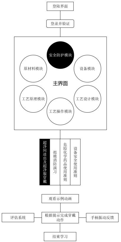
[0098] Embodiment 1 Wearing ultra-clean clothes and entering and exiting the ultra-clean room
[0099] Such as figure 2 As shown, the trainees put on the VR equipment, log in to the training system, enter the security protection module, and choose to enter and exit the clean room. Follow the system prompts to pass through the access control of the first dressing room, take off the jacket and put it in the wardrobe, and then enter the second dressing room. Wear ultra-clean clothes according to the animation example, and the sequence is: wear disposable gloves, disposable hair nets, disposable masks, ultra-clean clothes, ultra-clean caps, and ultra-clean shoes. After wearing, arrange the ultra-clean clothes in front of the mirror to ensure that they are dressed properly. Then follow the voice prompts to enter the air shower room, and leave the air shower room after air showering according to the regulations.
Embodiment 2
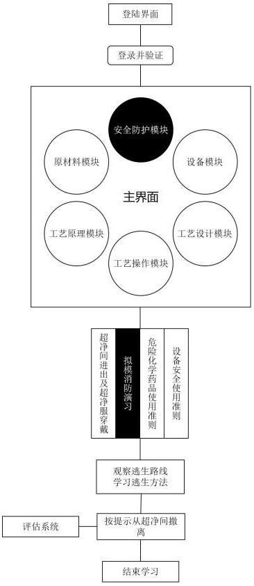
[0100] Embodiment 2 simulated fire drill
[0101] Such as image 3 As shown, the trainees put on the VR equipment, log in to the training system, enter the safety protection module, and select the fire drill. According to the system prompt, first observe the three-dimensional model of the clean room space and the escape route. After familiarizing yourself with the escape route, select the drill to begin. After the alarm sounds, quickly leave the clean room according to the escape route prompted by the system.
Embodiment 3
[0102] Embodiment 3 material observation
[0103] Such as Figure 4 As shown, the trainees put on the VR equipment, log in to the training system, enter the raw material module, and switch the scene to the material storage room. Find and open the substrate storage cabinet, take out the sample box, take out the virtual tweezers through the interactive button of the VR handle, and use the tweezers to pick up the four-inch single crystal silicon substrate from the sample box for observation. Move the four-inch monocrystalline silicon substrate to the center of the field of view, and its property parameters will be automatically displayed on the top of the substrate after one second, including: radius, thickness, conductivity type, doping elements and doping concentration, resistivity range, minority lifetime, Grain size, carbon and oxygen content, etc. After the observation, put the substrate back into the sample box, put the sample box back to its original place, and close the...
PUM
 Abstract
Description
Claims
Application Information


