Split gate power MOSFET device with highly doped layer and preparation method thereof

A split gate, highly doped technology, applied in semiconductor/solid-state device manufacturing, semiconductor devices, electric solid-state devices, etc. The effect of increasing the pressure capacity

Active Publication Date: 2020-11-10
INST OF MICROELECTRONICS CHINESE ACAD OF SCI
View PDF4 Cites 1 Cited by
  • Summary
  • Abstract
  • Description
  • Claims
  • Application Information

AI Technical Summary

Problems solved by technology

[0004] In view of the above-mentioned analysis, the present invention aims to provide a split-gate power MOSFET device with a highly doped layer and its preparation method, in order to solve the inability of the prior art The problem of further reducing the on-state resistance of the device while increasing the breakdown voltage

Method used


Image

  • Split gate power MOSFET device with highly doped layer and preparation method thereof
  • Split gate power MOSFET device with highly doped layer and preparation method thereof
  • Split gate power MOSFET device with highly doped layer and preparation method thereof

Examples


Embodiment 1

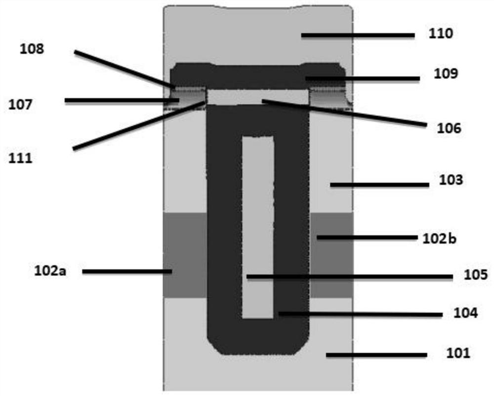
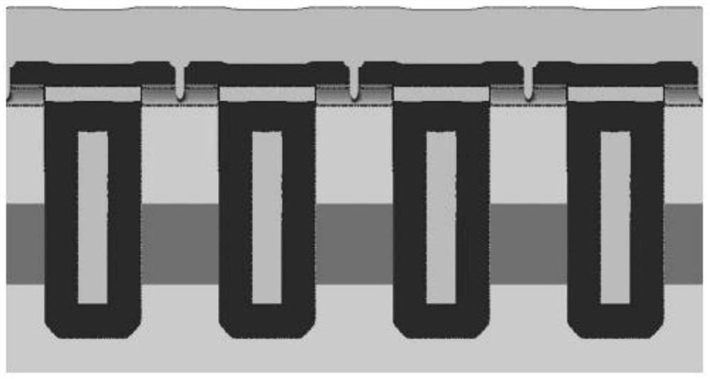
[0052] A specific embodiment of the present invention discloses a split gate power MOSFET device with a highly doped layer, such as figure 1 As shown, the conduction region of the MOSFET device includes several primitive cells arranged periodically, each of which includes a trench, a shielding electrode 105 and a trench gate electrode 106 . Wherein, the trench is disposed in the epitaxial layer of the semiconductor substrate of the first conductivity type; the shielding electrode is disposed in the trench, and the trench gate electrode is disposed on the top of the trench; the Both the shielding electrode and the trench gate electrode are made of the second conductivity type material, and are separated from each other by a dielectric layer; the epitaxial layer is made of the first conductivity type material, including doped and doped layers sequentially stacked on the semiconductor substrate The first epitaxial layer 101, the second epitaxial layer (102a, 102b) and the third e...

Embodiment 2

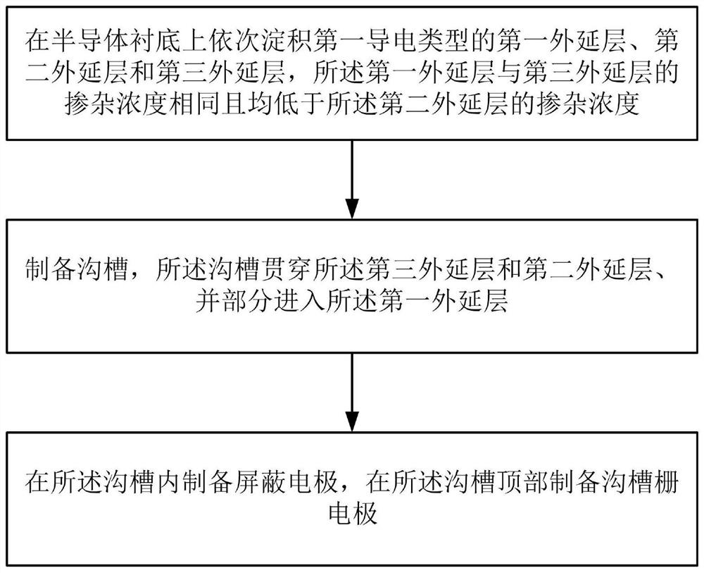
[0066] Another specific embodiment of the present invention discloses a method for preparing the split gate power MOSFET device with a highly doped layer described in Embodiment 1, the flow chart is as follows image 3 As shown, the steps are as follows:

[0067] Step S1: sequentially depositing a first epitaxial layer, a second epitaxial layer and a third epitaxial layer of the first conductivity type on the semiconductor substrate, the first epitaxial layer and the third epitaxial layer have the same and low doping concentration a doping concentration in the second epitaxial layer;

[0068] Step S2: preparing a trench, the trench penetrates the third epitaxial layer and the second epitaxial layer, and partially enters the first epitaxial layer;

[0069] There are many ways to form grooves. In this embodiment, the grooves are specifically formed by a photolithography process;

[0070] Step S3: preparing a shielding electrode in the trench, and preparing a trench gate electr...


PUM

PropertyMeasurementUnit
thicknessaaaaaaaaaa
thicknessaaaaaaaaaa

Abstract

The invention relates to a split gate power MOSFET device with a highly doped layer and a preparation method thereof, belongs to the field of semiconductor devices, and solves the problem that the on-state resistance of the device cannot be further reduced while the breakdown voltage is improved in the prior art. An MOSFET device conduction region comprises a plurality of primitive cells arrangedperiodically, and each primitive cell comprises a trench, a shielding electrode and a trench gate electrode. The trench is arranged in an epitaxial layer of the semiconductor substrate, the shieldingelectrode is arranged in the trench, and the trench gate electrode is arranged at the top of the trench. The shielding electrode and the trench gate electrode are both made of second conductive type materials, the epitaxial layer is made of a first conductive type material and comprises a first epitaxial layer, a second epitaxial layer and a third epitaxial layer which are sequentially stacked onthe semiconductor substrate and have the same doping type, and the doping concentration of the first epitaxial layer and the doping concentration of the third epitaxial layer are the same and are lower than the doping concentration of the second epitaxial layer. According to the MOSFET device, the on-resistance of the device is further reduced while the breakdown voltage is improved, and the FOM value of the device is improved.

Description

technical field [0001] The invention relates to the technical field of semiconductor devices, in particular to a split gate power MOSFET device with a highly doped layer and a preparation method thereof. Background technique [0002] With the development of power electronic systems, the power MOSFET (Metal Oxide Semiconductor Field Effect Transistor) device plays an increasingly important role due to its excellent performance, and has become one of the irreplaceable important devices in the field of microelectronics. However, due to the existence of "silicon limit", the development of power MOSFET devices is seriously hindered. [0003] B.J.Baliga reported a charge-coupled power MOSFET that uses the charge balance effect to reduce the on-resistance in 1997, known as the split-gate trench MOSFET. This structure can greatly reduce the on-resistance of the device, but the electric field distribution in the drift region of this structure is not very ideal. This situation is pa...

Claims


Application Information

Patent Timeline
Patent Type & Authority Applications(China)
IPC IPC(8): H01L29/786H01L29/06H01L23/552H01L21/336H01L27/088
CPCH01L29/78606H01L29/78642H01L29/0623H01L29/66742H01L23/552H01L27/088
Inventor 陈润泽王立新
Owner INST OF MICROELECTRONICS CHINESE ACAD OF SCI
Why Eureka
Try Eureka