Semiconductor structure and manufacturing method thereof
A manufacturing method and semiconductor technology, applied in the fields of semiconductor/solid-state device manufacturing, electrical components, circuits, etc., can solve problems such as trench voids, and achieve the effect of improving process efficiency
- Summary
- Abstract
- Description
- Claims
- Application Information
AI Technical Summary
Problems solved by technology
Method used
Image

Examples
Embodiment 1
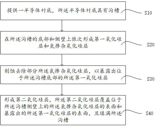
[0036] The following is attached Figure 2-8 The semiconductor structure manufacturing method provided by the embodiment of the present invention is described in detail.
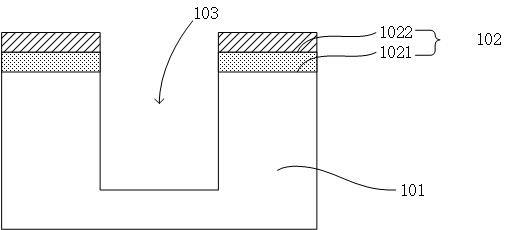
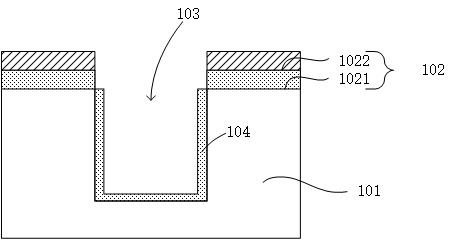
[0037] First, execute step S10, please refer to figure 2 , providing a semiconductor substrate 101 having several trenches 103 . To simplify, figure 2 Only one groove is shown in .
[0038] The semiconductor substrate 101 may be monocrystalline silicon or polycrystalline silicon, or semiconductor materials such as silicon, germanium, silicon germanium, gallium arsenide, or a composite structure such as silicon-on-insulator. Those skilled in the art can select the type of the semiconductor substrate 101 according to the semiconductor devices formed on the semiconductor substrate 101 , so the type of the semiconductor substrate 101 should not limit the protection scope of the present invention.
[0039] In a specific embodiment, the trench 103 serves as an isolation structure to provide isolation for the...
Embodiment 2
[0071] The difference from Embodiment 1 is that in step S20, the nitrogen-doped silicon oxide layer 105 is formed by an NO annealing process, and the NO annealing process is formed by gas NO and SiO in the first silicon oxide layer 104 2 reaction to generate SiO x N y , in this embodiment, the nitrogen-doped silicon oxide layer 105 is SiO x N y .
[0072] In the NO annealing process, the temperature of the annealing treatment can be set according to actual needs. Preferably, in this embodiment, the temperature of the annealing treatment is 800°C-1100°C.
[0073] In the NO annealing process, the time for the annealing treatment can be set according to actual needs. Preferably, in this embodiment, the time for the annealing treatment is less than 70s.
[0074] In the NO annealing process, the pressure of the annealing treatment can be set according to actual needs. Preferably, in this embodiment, the pressure of the annealing treatment is 500 torr-1000 torr.
[0075] In the...
PUM
 Abstract
Description
Claims
Application Information