
LD multispectral exposure method and system for solder mask circuit integrated exposure

An exposure method and exposure system technology, applied in the field of LD multi-spectral exposure method and system for integrated exposure of solder resist lines, can solve problems such as loss of gloss on the surface of solder resist boards, and achieve system depth of field, high laser monochromaticity, good exposure performance

Inactive Publication Date: 2020-11-17
ZHONGSHAN AISCENT TECH
View PDF4 Cites 2 Cited by
  • Summary
  • Abstract
  • Description
  • Claims
  • Application Information

AI Technical Summary

Problems solved by technology

[0005] For this reason, the embodiment of the present invention provides an LD multi-spectral exposure method and system for integrated exposure of solder resist lines to solve the problem of solder resist caused by the application of single-wavelength laser direct exposure equipment to the solder resist process in the prior art. The problem of losing gloss on the surface of the board

Method used


Image

  • LD multispectral exposure method and system for solder mask circuit integrated exposure
  • LD multispectral exposure method and system for solder mask circuit integrated exposure
  • LD multispectral exposure method and system for solder mask circuit integrated exposure

Examples


Embodiment 1

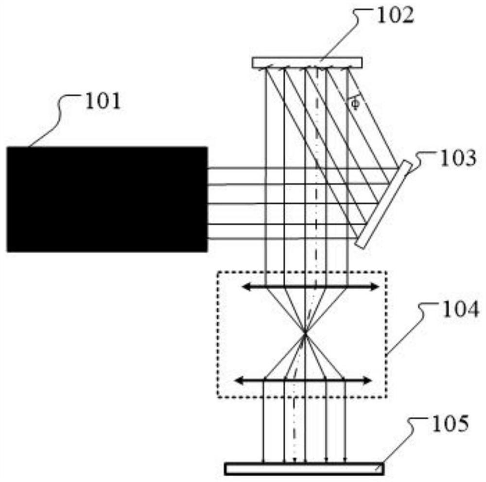
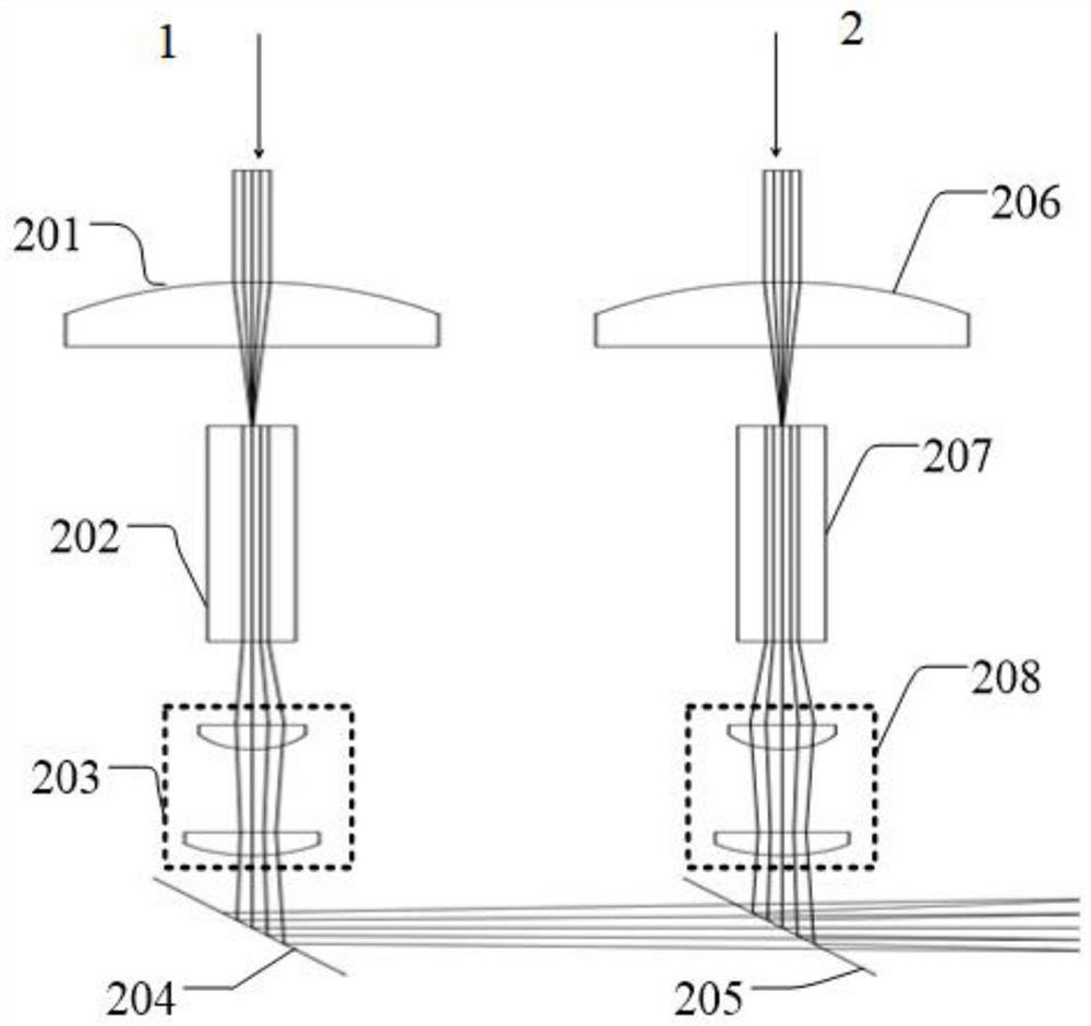
[0025] Embodiment 1: An LD multispectral exposure system for integrated exposure of solder resist lines, such as figure 1 As shown, it includes a combined light illumination system 101 that combines several light sources with different wavelengths, a spatial light modulator 102, a redirection element, and a wide-spectrum imaging system 104. In this embodiment, the above-mentioned redirection element is preferably a reflective The mirror 103 can also be set as other devices that change the direction of light propagation, such as reflective prisms, etc. The above-mentioned light-combining lighting system 101 is used to combine two LD lights of different wavelengths to combine light, and the light passing through the light-combining lighting system 101 Reflected by the mirror 103 to the spatial light modulator 102 , the spatial light modulator 102 converts the digital signal into an optical signal and projects it through graphic modulation, and then forms an image on the exposure ...

Embodiment 2

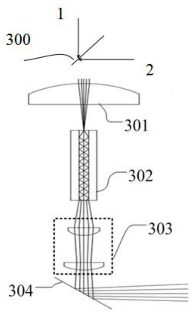
[0028] Embodiment 2: The difference with Embodiment 1 is that, as image 3 As shown, in this embodiment, the combined light illumination system 101 sequentially includes a dichroic filter 300, a third coupling element 301, a third light homogenizing element 302, a third focusing shaping mirror group 303, and a third dichroic mirror from the light source path. 304, the first light source 1 and the second light source 2 combine light through the dichroic filter 300 to form a multi-wavelength mixed light source, after being coupled by the third coupling member 301, it enters the third light homogenizing member 302, passes through the third The mixed light from the homogenizing element 302 forms a complete illumination spot after the third focusing and shaping mirror group 303, and irradiates on the third beam splitter 304, and the third beam splitter 304 that changes the light propagation route can be selected according to the needs in the optical path process According to the di...

Embodiment 3

[0029] Embodiment 3: The difference with Embodiment 1 and Embodiment 2 is that, as Figure 4 As shown, in this embodiment, the combined light illumination system 101 includes a first optical fiber, a second optical fiber and a fourth focusing shaping mirror group 402, the first light source 1 is incident into the first optical fiber, and the second light source 2 is incident into the second In the optical fiber, the first light source 1 and the second light source 2 are respectively coupled and combined by optical fiber to complete the light uniformity and shaping process, and are directly processed at the optical fiber outlet 401 to form the desired shape, and then formed by the fourth focusing and shaping mirror group 402 to form an ideal The lighting spot is enough.


PUM


Abstract

The embodiment of the invention discloses an LD multispectral exposure method for solder mask circuit integrated exposure. The LD multispectral exposure method comprises the following steps: S1, carrying out combined light combination on a plurality of LD light rays with different wavelengths; S2, reflecting the combined light to a spatial light modulator through a reflector; S3, converting the digital signal into an optical signal by a spatial light modulator through graphic modulation; and S4, light rays projected by the spatial light modulator being imaged on an exposure plate through a wide-spectrum imaging system, two or more lasers being used as light sources of exposure equipment by combining the lasers with different wavelengths, two or more lasers being used as light sources of the equipment which can ensure that the numerical aperture of the system is small and the imaging quality is high. The laser monochromaticity is high, and the exposure performance is good. The depth offield of the system is large, and the product yield is guaranteed. Therefore, the imaging quality of the system can meet the requirements of the circuit process, and the equipment not only meets the solder mask process, but also has the capability of circuit production.

Description

technical field [0001] Embodiments of the present invention relate to the technical field of circuit solder mask exposure in digital lithography, and in particular to an LD multispectral exposure method and system for integrated exposure of solder mask circuits. Background technique [0002] The photolithography process of the circuit board can be divided into two parts according to the process: line or character layer exposure, solder mask exposure, the solder mask is a layer of solder mask on the surface of the printed circuit board, to prevent the surface of the circuit board from Oxidation occurs, and the preparation of the solder resist layer. The traditional exposure process is completed by exposing the surface of the film with a light source. The light source is generally a high-pressure mercury lamp or an array LED. The wavelength of the light source is generally 350nm-410nm. The solder resist materials currently used in the industry are also Generally, the photosens...

Claims


Application Information

Patent Timeline
Patent Type & Authority Applications(China)
IPC IPC(8): H05K3/06G03F7/20
CPCG03F7/20H05K3/06
Inventor 徐珍华梅文辉王瑞汪孝军劳仲标
Owner ZHONGSHAN AISCENT TECH
Learn More