Manufacturing method of super junction device

A manufacturing method and super junction technology, applied in semiconductor/solid-state device manufacturing, semiconductor devices, electrical components, etc., can solve problems such as reducing device performance, and achieve the effect of reducing the impact

Active Publication Date: 2020-11-27
SHANGHAI HUAHONG GRACE SEMICON MFG CORP
View PDF10 Cites 2 Cited by
  • Summary
  • Abstract
  • Description
  • Claims
  • Application Information

AI Technical Summary

Problems solved by technology

[0020] It can be seen from the above that in the existing method, 10 photolithography processes are required. After the super junction is formed, there are many subsequent thermal processes. Therefore, the super junction formed by the existing method is easily affected by the thermal process and will produce a large Interdiffusion, which can degrade the performance of the device

Method used


Image

  • Manufacturing method of super junction device
  • Manufacturing method of super junction device
  • Manufacturing method of super junction device

Examples


Embodiment Construction

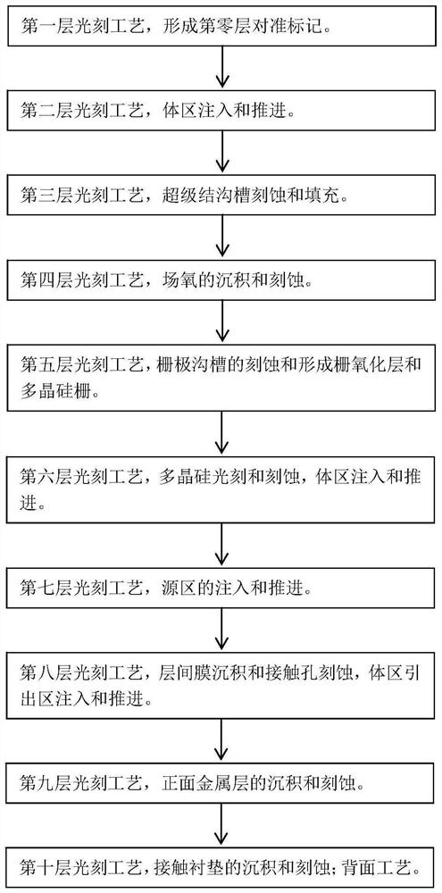
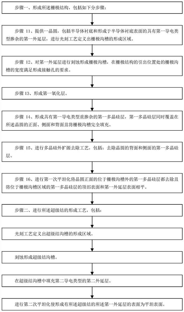
[0108] The manufacturing method of the super junction device of the embodiment of the present invention:

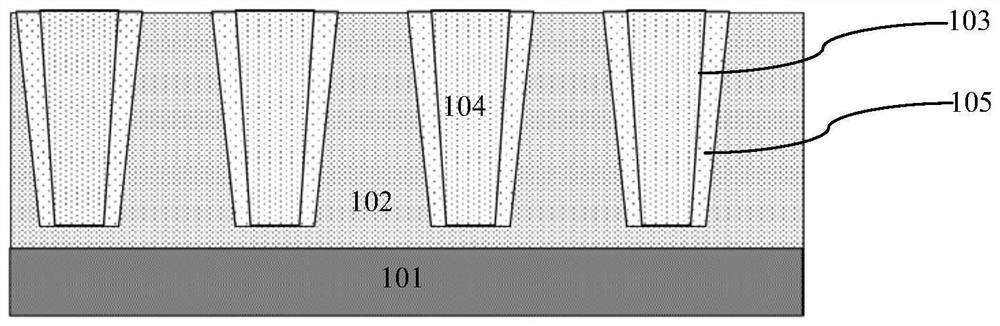
[0109] In the manufacturing method of the super junction device in the embodiment of the present invention, the super junction device includes a super junction, and the structure schematic diagram of the super junction device please refer to Figure 5Q As shown, in the device unit area, the device front unit structure of the super junction device is formed on the super junction; the device front unit structure includes a gate structure, a body region 5 of the second conductivity type, a first conductivity type heavily doped impurity source region 6, field oxygen 8, interlayer film 9, contact hole 10, front metal layer 11; the super junction is formed by alternating columns of the first conductivity type and the second conductivity type, and one of the first conductivity type A column of a conductivity type and an adjacent column of the second conductivity type form a supe...


PUM

PropertyMeasurementUnit
thicknessaaaaaaaaaa

Abstract

The invention discloses a manufacturing method of a super junction device, which comprises the steps of 1, forming a gate structure, specifically, forming a gate trench, a first oxide layer and a first polycrystalline silicon layer, removing the first polycrystalline silicon layer on the side surface and the back surface of a wafer, and carrying out primary planarization to remove the first polycrystalline silicon layer on the front surface of the wafer outside the gate trench; and 2, forming a super junction in the first epitaxial layer with the flat surface on which the trench gate is formed, wherein in the forming process of the super junction, a second epitaxial layer is adopted to fill the super junction trench, and then secondary planarization is performed so as to enable the surfaceof the first epitaxial layer with the super junction to be a flat surface. According to the invention, the full-flat process can be realized, the trench gate process can be conveniently arranged before the super junction forming process, and the thermal process after the super junction is formed can be reduced, so that the mutual diffusion of impurities of the super junction is reduced, the device performance is improved, a photomask can be saved, and the process cost is reduced; and the influence of polycrystalline silicon residues on the charge balance of the super junction can be prevented.

Description

technical field [0001] The invention relates to a method for manufacturing a semiconductor integrated circuit, in particular to a method for manufacturing a super junction device. Background technique [0002] The super junction is composed of alternately arranged P-type thin layers also called P-type pillars (Pillar) and N-type thin layers also called N-type pillars formed in the semiconductor substrate. Devices using super junctions are super junction devices such as super junction devices. junction MOSFET. The internal reduced surface electric field (Resurf) technology using P-type thin layer and N-type thin layer charge balance can increase the reverse breakdown voltage of the device while maintaining a small on-resistance. [0003] The pillar structure of the PN interval of the super junction is the biggest feature of the super junction. Currently, there are mainly two methods for manufacturing the pillar structure of the PN spacer, one is obtained by multiple epitaxy...

Claims


Application Information

Patent Timeline
Patent Type & Authority Applications(China)
IPC IPC(8): H01L21/336H01L29/78H01L29/06
CPCH01L29/66734H01L29/7813H01L29/0634Y02P70/50
Inventor 李昊
Owner SHANGHAI HUAHONG GRACE SEMICON MFG CORP
Why Eureka
Try Eureka