Manufacturing method of super junction device

A manufacturing method and super junction technology, applied in semiconductor/solid-state device manufacturing, semiconductor devices, electrical components, etc., can solve problems such as reducing device performance, and achieve the effect of improving performance

Pending Publication Date: 2020-11-24
SHANGHAI HUAHONG GRACE SEMICON MFG CORP
View PDF4 Cites 5 Cited by
  • Summary
  • Abstract
  • Description
  • Claims
  • Application Information

AI Technical Summary

Problems solved by technology

[0020] It can be seen from the above that in the existing method, 10 photolithography processes are required. After the super junction is formed, there are many subsequent thermal processes. Therefore, the super junction formed by the existing method is easily affected by the thermal process and will produce a large Interdiffusion, which can degrade the performance of the device

Method used


Image

  • Manufacturing method of super junction device
  • Manufacturing method of super junction device
  • Manufacturing method of super junction device

Examples


Embodiment Construction

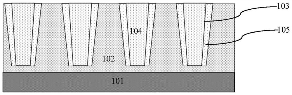
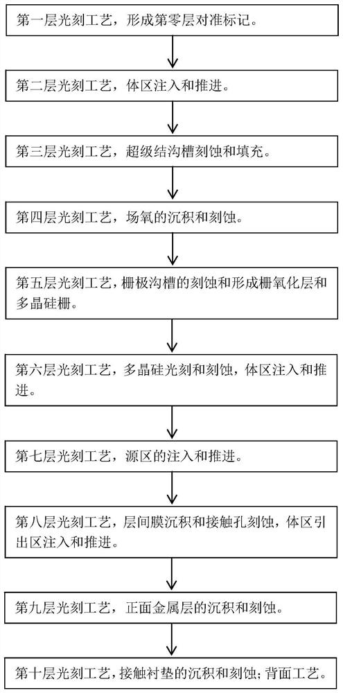
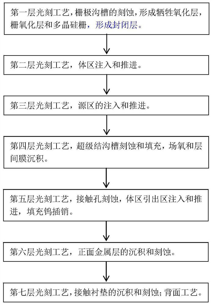
[0097] Such as image 3 Shown is a flowchart of a method for manufacturing a super junction device according to an embodiment of the present invention; image 3 is described according to the lithography process level, a lithography process level includes multiple specific process steps, and a lithography process level only performs the lithography process corresponding to one mask. Such as Figure 4A to Figure 4N Shown is a schematic diagram of the device structure in each step of the manufacturing method of the super junction device in the embodiment of the present invention; the manufacturing method of the super junction device in the embodiment of the present invention includes steps:

[0098] Step 1, forming the gate structure, the gate structure is a trench gate, and the formation process of the trench gate includes:

[0099] A first epitaxial layer 2 with a first conductivity type is provided, and a photolithography process is performed to define a formation region of ...


PUM

PropertyMeasurementUnit
thicknessaaaaaaaaaa

Abstract

The invention discloses a manufacturing method of a super junction device. The manufacturing method comprises the steps: step 1, filling a gate electrode trench with a polysilicon gate and carrying out first planarization to form a gate electrode structure; step 2, etching back the polysilicon gate and forming a sealing layer in a top recess formed by back etching; and step 3, filling the super junction trench with a second epitaxial layer and carrying out secondary planarization to form a super junction. According to the invention, a full-flat process can be realized, the trench gate processcan be conveniently arranged before the super junction forming process, and the thermal process after the super junction is formed can be reduced, so that the mutual diffusion of impurities of the super junction is reduced, the device performance is improved, a photomask can be saved, and the process cost is reduced; and doping and external expansion of the polysilicon gate can be prevented, a gate oxide layer can be protected, and the product quality and reliability can be improved.

Description

technical field [0001] The invention relates to a method for manufacturing a semiconductor integrated circuit, in particular to a method for manufacturing a super junction device. Background technique [0002] The super junction is composed of alternately arranged P-type thin layers also called P-type pillars (Pillar) and N-type thin layers also called N-type pillars formed in the semiconductor substrate. Devices using super junctions are super junction devices such as super junction devices. junction MOSFET. The internal reduced surface electric field (Resurf) technology using P-type thin layer and N-type thin layer charge balance can increase the reverse breakdown voltage of the device while maintaining a small on-resistance. [0003] The pillar structure of the PN interval of the super junction is the biggest feature of the super junction. Currently, there are mainly two methods for manufacturing the pillar structure of the PN spacer, one is obtained by multiple epitaxy...

Claims


Application Information

Patent Timeline
Patent Type & Authority Applications(China)
IPC IPC(8): H01L21/336H01L29/78H01L29/06
CPCH01L29/66734H01L29/7813H01L29/0634
Inventor 李昊
Owner SHANGHAI HUAHONG GRACE SEMICON MFG CORP
Why Eureka
Try Eureka