Supercharge Your Innovation With Domain-Expert AI Agents!

Method for transferring porous PDMS film in organ chip

An organ chip and thin film technology, applied in the field of micromachining, can solve the problems of complicated operation, increased experimental difficulty, low success rate, etc., and achieve the effect of simple operation steps and good repeatability

Pending Publication Date: 2020-12-01
UNIV OF SCI & TECH OF CHINA
View PDF0 Cites 2 Cited by
  • Summary
  • Abstract
  • Description
  • Claims
  • Application Information

AI Technical Summary

Problems solved by technology

This method is complicated to operate and has a low success rate
There is a sacrificial layer method that requires an additional sacrificial layer material to assist the transfer. Among them, the photoresist is directly used as a sacrificial layer to transfer the PDMS film, but this method requires PDMS to be soaked in acetone for a long time, which will deform the PDMS, and Photoresist generally has a lot of residue
There is also the use of PAA (polyacrylic acid), a water-soluble material, as a sacrificial layer to realize the transfer. Although this method can transfer the film without residue, because it is a water-soluble material, the PDMS film cannot be soaked when the through hole is prepared by patterning in the early stage. In aqueous solution, this greatly increases the experimental difficulty

Method used


Image

  • Method for transferring porous PDMS film in organ chip
  • Method for transferring porous PDMS film in organ chip
  • Method for transferring porous PDMS film in organ chip

Examples


Embodiment 1

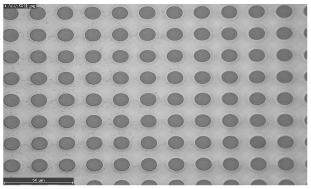
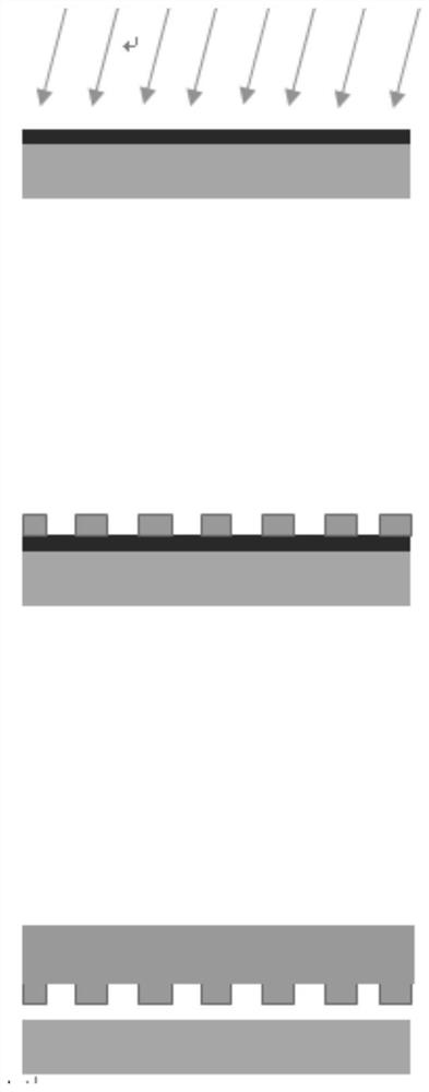
[0075] Firstly, the photoresist S1813 is spin-coated on the silicon wafer substrate, and the parameter is 3000rpm, 40s. It was then baked and cured at 115°C for 90s. Then use UV lithography SUSSMA6 for flood exposure, the exposure time is 1-2s longer than usual, and the photoresist with fully broken chain can be obtained by exposing for 9s with this equipment.

[0076] Surface O of the photoresist using a glue remover 2 Plasma treatment, O 2 The flow rate is 30sccm, the radio frequency power is 30w, and the surface treatment time is 2min, then the PDMS film is spin-coated with a thickness of 5μm, and baked and cured at 120°C for 40min. Then, the PDMS thin film is photolithographically patterned into a through-hole structure by using a microfabrication process.

[0077] The graphical process is: first use RIE to treat the PDMS surface with oxygen plasma, and the parameter is O 2 The flow rate is 30sccm, the radio frequency power is 200w, and the processing time is 2min. Th...

Embodiment 2

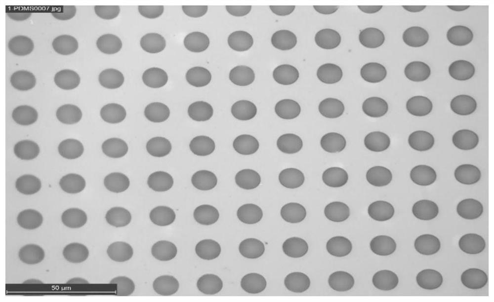
[0080] Firstly, the photoresist S1813 is spin-coated on the silicon wafer substrate, and the parameter is 3000rpm, 40s. It was then baked and cured at 115°C for 90s. Then use UV lithography SUSSMA6 for flood exposure, the exposure time is 1-2s longer than usual, and the photoresist with fully broken chain can be obtained by exposing for 9s with this equipment.

[0081] Surface O of the photoresist using a glue remover 2 Plasma treatment, O 2 The flow rate is 30sccm, the radio frequency power is 30w, and the surface treatment time is 2min, then the PDMS film is spin-coated with a thickness of 10μm, and baked and cured at 120°C for 40min. Then, the PDMS thin film is photolithographically patterned into a through-hole structure by using a microfabrication process.

[0082] The graphical process is: first use RIE to treat the PDMS surface with oxygen plasma, and the parameter is O 2 The flow rate is 30sccm, the radio frequency power is 200w, and the processing time is 2min. T...


PUM

PropertyMeasurementUnit
Thicknessaaaaaaaaaa

Abstract

The invention provides a method for transferring a porous PDMS film in an organ chip, which comprises the following steps: spin-coating photoresist on a substrate, and exposing the photoresist; carrying out surface oxygen plasma treatment on the exposed photoresist, spin-coating a PDMS film on the photoresist, and curing; photoetching and patterning the cured PDMS thin film; bonding the patternedPDMS film with an upper channel of the organ chip, and placing the bonded combined module in a developing solution for ultrasonic treatment, so as to transfer the PDMS film to the upper channel of theorgan chip. According to the invention, the photoresist after extensive exposure is used as the sacrificial layer to transfer the PDMS film, so that the photoresist can be fully dissolved in the developing solution after the PDMS film is bonded with the upper-layer channel of the organ chip, thereby realizing the transfer of the film. And an acetone organic solvent soaking mode is not adopted, and photoresist residues are avoided. The method is compatible with a conventional semiconductor processing technology, the operation steps are simple, and the repeatability is good.

Description

technical field [0001] The invention relates to the technical field of micromachining, in particular to a method for transferring a porous PDMS film in an organ chip. Background technique [0002] Human organ chips, such as lung organ chip models, mainly include upper and lower channel modules and a layer of PDMS porous film in between. It can be used to simulate the cell behavior in the microenvironment of tissues and organs related to the human body in vitro, which is of great significance for the study of human physiology and pathology. Therefore, it is very important to study the model of the organ chip, and the successful transfer of the middle PDMS film to the upper channel is one of the difficulties. [0003] There are mainly two ways for the transfer of PDMS thin films, which can be divided into those without sacrificial layer and those with sacrificial layer. The non-sacrificing layer is mainly achieved by silanizing the substrate of the PDMS film, generally a PDM...

Claims


Application Information

Patent Timeline
IPC IPC(8): B81C1/00
CPCB81C1/00015B81C1/00158B81C2201/019
Inventor 陈陈周成刚
Owner UNIV OF SCI & TECH OF CHINA
Features
  • R&D
  • Intellectual Property
  • Life Sciences
  • Materials
  • Tech Scout
  • Unparalleled Data Quality
  • Higher Quality Content
  • 60% Fewer Hallucinations
Learn More