Preparation method of graphene transparent conductive film with superfine conductive pattern
A technology of transparent conductive film and conductive pattern, applied in cable/conductor manufacturing, conductive layer on insulating carrier, circuit, etc., can solve the problems of high manufacturing cost, difficult to meet, low transmittance, etc., and achieve excellent performance performance effect
- Summary
- Abstract
- Description
- Claims
- Application Information
AI Technical Summary
Problems solved by technology
Method used
Image

Examples
Embodiment 1
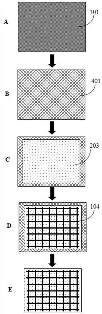
[0043] There is the preparation method of the graphene transparent conductive film (without protective film) of superfine conductive pattern, see image 3 , the process flow A-E are respectively: A, preparation of glass substrate; B, preparation of parylene coating; C, preparation of polyimide film; D, preparation of graphene pattern on polyimide film for LIG process; E , Peel off ultra-thin, flexible graphene transparent conductive film. Specific steps are as follows:
[0044] 1) Prepare a flat panel display glass 301 with a glass thickness of 1 mm, and clean and dry it for use (step A).
[0045] 2) Deposit a layer of parylene film 401 with a thickness of 5 microns on the surface of the flat glass by chemical vapor deposition as a release film (step B).
[0046] 3) On the surface of the parylene film 401, a layer of polyimide (PI) transparent insulating film 203 is prepared by suspension coating polyimide prepolymer by suspension coating method, and then undergoes high-temp...
Embodiment 2
[0050] The preparation method of the graphene transparent conductive film (without protective film) of superfine conductive pattern:
[0051] 1) Prepare a flat panel display glass with a glass thickness of 1 mm, and clean and dry it for later use;
[0052] 2) Deposit a layer of parylene film with a thickness of 5 microns on the surface of the flat glass as a release film by chemical vapor deposition;
[0053] 3) On the surface of the parylene film, a layer of polyimide (PI) transparent insulating film was prepared by suspension coating method by suspension coating polyimide prepolymer, and then imidized at high temperature, with a film thickness of 5 Micron, imidization condition: 300°C, 60min;
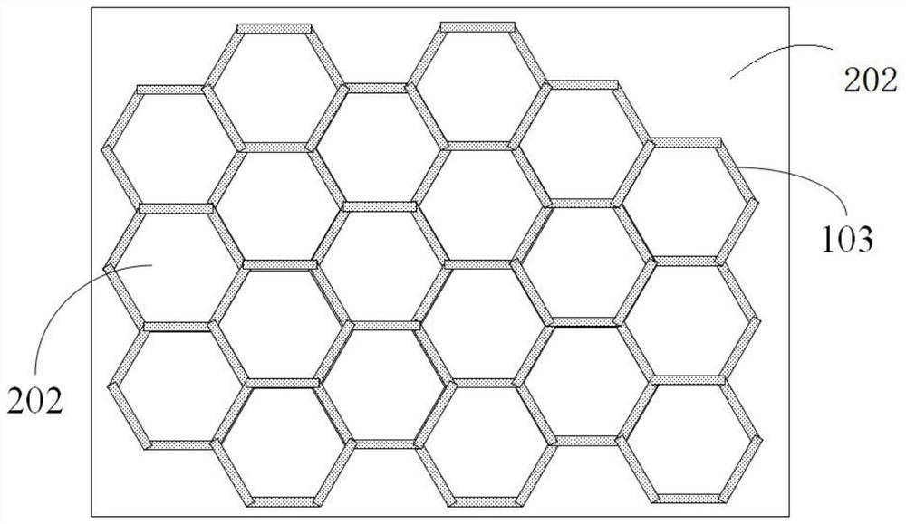
[0054] 4) Using laser-induced (LIG) graphene processing technology with a short-wavelength laser light source, graphene is prepared on the surface of the transparent insulating film and a fine graphene pattern (honeycomb shape) is formed. The internal structure of the pattern is show...
Embodiment 3
[0057] The preparation method of the graphene transparent conductive film (with protective film) with ultra-fine conductive pattern:
[0058] 1) Prepare a flat panel display glass with a glass thickness of 1 mm, and clean and dry it for later use;
[0059] 2) Deposit a layer of parylene film with a thickness of 10 microns on the surface of the flat glass as a release film by chemical vapor deposition;
[0060] 3) On the surface of the parylene film, the polyimide prepolymer is coated by the slit coating method, and then a layer of polyimide (PI) transparent insulating film is prepared through high-temperature imidization, and the film thickness is 15 microns, the imidization conditions are: 300°C, 60min;
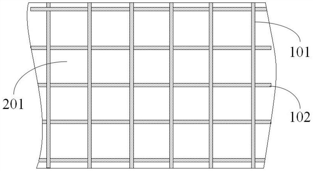
[0061] 4) Using laser-induced (LIG) graphene processing technology with a short-wavelength laser light source, graphene is prepared on the surface of the transparent insulating film and a fine graphene pattern (square shape) is formed. In a single graphene grid, the wires ...
PUM
| Property | Measurement | Unit |
|---|---|---|
| Thickness | aaaaa | aaaaa |
| Thickness | aaaaa | aaaaa |
| Thickness | aaaaa | aaaaa |
Abstract
Description
Claims
Application Information
 - R&D
- Intellectual Property
- Life Sciences
- Materials
- Tech Scout
- Unparalleled Data Quality
- Higher Quality Content
- 60% Fewer Hallucinations
Browse by: Latest US Patents, China's latest patents, Technical Efficacy Thesaurus, Application Domain, Technology Topic, Popular Technical Reports.
© 2025 PatSnap. All rights reserved.Legal|Privacy policy|Modern Slavery Act Transparency Statement|Sitemap|About US| Contact US: help@patsnap.com