Preparation method for improving performance of SOI device

A performance and device technology, which is applied in the field of preparation to improve the performance of SOI devices, can solve problems such as high consumption of insulating silicon, alignment deviation, and contact hole perforation, so as to solve alignment deviation, reduce consumption, and avoid pinching. wearing effect

Pending Publication Date: 2020-12-04
SHANGHAI HUALI INTEGRATED CIRCUTE MFG CO LTD
View PDF0 Cites 0 Cited by
  • Summary
  • Abstract
  • Description
  • Claims
  • Application Information

AI Technical Summary

Problems solved by technology

[0006] In view of the above-mentioned shortcomings of the prior art, the object of the present invention is to provide a preparation method for improving the performance of SOI devices, which is used to solve the problem of contact hole perforation caused by excessive consumption of insulating silicon in the preparation of fully depleted insulator devices in the prior art. , and the problem of alignment shift caused by thermal expansion during photolithography

Method used


Image

  • Preparation method for improving performance of SOI device
  • Preparation method for improving performance of SOI device
  • Preparation method for improving performance of SOI device

Examples


Embodiment Construction

[0033] The embodiments of the present invention are described below through specific specific examples, and those skilled in the art can easily understand other advantages and effects of the present invention from the contents disclosed in this specification. The present invention can also be implemented or applied through other different specific embodiments, and various details in this specification can also be modified or changed based on different viewpoints and applications without departing from the spirit of the present invention.

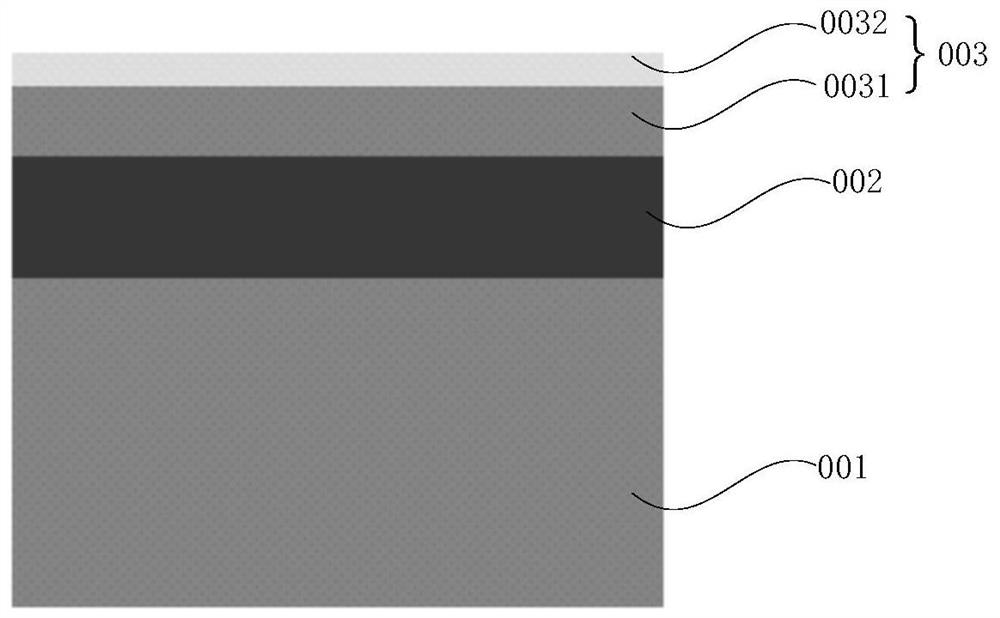
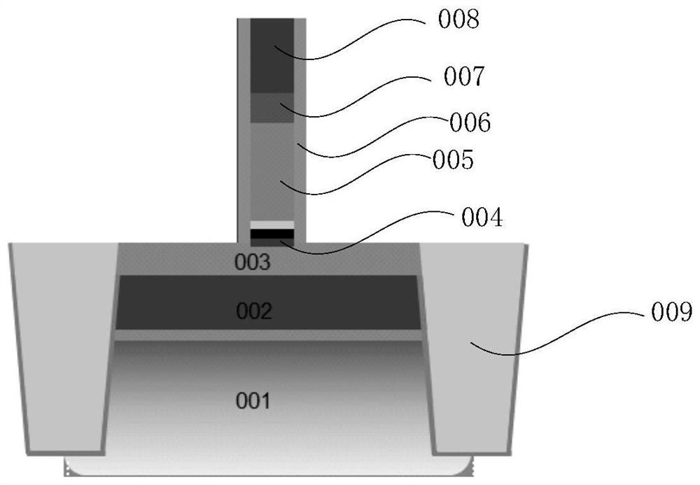
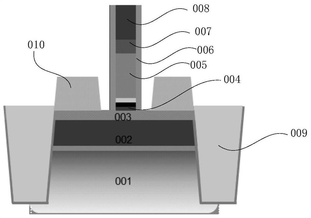
[0034] see Figure 1 to Figure 6 . It should be noted that the drawings provided in this embodiment are only to illustrate the basic concept of the present invention in a schematic way, so the drawings only show the components related to the present invention rather than the number, shape and the number of components in actual implementation. For dimension drawing, the type, quantity and proportion of each component can be changed at will i...


PUM

PropertyMeasurementUnit
thicknessaaaaaaaaaa

Abstract

The invention provides a preparation method for improving the performance of an SOI device, and the method comprises the steps of providing an SOI structure which comprises matrix silicon, a buried oxide layer located on the matrix silicon and surface silicon located on the buried oxide layer, forming a silicon film layer with the thickness of 2nm on the surface silicon, and enabling the silicon film layer and the surface silicon to form an insulating silicon layer; enabling part of the insulating silicon layer on the surface of the SOI structure to react to form a silicon oxide film layer; and forming a pseudo gate structure of a PMOS on the silicon oxide thin film layer, wherein the pseudo gate at least comprises a gate oxide layer, a polycrystalline silicon layer located above the gateoxide layer, and a first side wall attached to the side wall of the polycrystalline silicon layer. By adopting epitaxial silicon growth and a furnace tube process, on one hand, the consumption of insulating silicon can be reduced, germanium-silicon growth is facilitated, and a contact hole is prevented from being punctured; on the other hand, the problem of alignment offset caused in the photoetching process is solved, contact hole offset is avoided, and the device can work normally.

Description

technical field [0001] The invention relates to the technical field of semiconductors, in particular to a preparation method for improving the performance of an SOI device. Background technique [0002] With the development of silicon integrated circuit technology, many methods are used to improve device performance. Fully depleted silicon-on-insulator has an ultra-thin insulating layer (buried oxide layer), which can realize dielectric isolation of components in integrated circuits and completely eliminate the latch-up effect in substrate silicon CMOS circuits. Among them, fully depleted silicon-on-insulator devices are considered to be a promising new type of planar devices due to their low power consumption, high speed, high integration density, and simple process. [0003] In the manufacturing process of fully depleted silicon-on-insulator (FD-SOI) devices, the source and drain electrodes of PMOS are grown on silicon-on-insulator (SOI) silicon germanium (SIGE). (SOI). ...

Claims


Application Information

Patent Timeline
Patent Type & Authority Applications(China)
IPC IPC(8): H01L21/336H01L21/768
CPCH01L21/76877H01L29/66545H01L29/66568H01L2221/1068
Inventor 唐霞王昌锋廖端泉
Owner SHANGHAI HUALI INTEGRATED CIRCUTE MFG CO LTD
Why Eureka
Try Eureka