An Electrically Controlled Active Coupled Cavity Laser
A coupled cavity and electrical regulation technology, applied in the visible light field, can solve the problems of poor GaN microcavity laser characteristics, and achieve the effect of improving electrical regulation effect, practicability and convenience.
- Summary
- Abstract
- Description
- Claims
- Application Information
AI Technical Summary
Problems solved by technology
Method used
Image
Examples
preparation example Construction
[0032] Such as Figure 4 As shown, a preparation method of an electrically regulated active coupled cavity laser comprises the following steps:
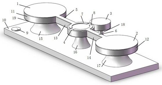
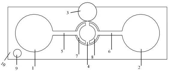
[0033] The first step: Spin-coat photoresist on the upper surface of GaN on the silicon-based GaN wafer, and then use optical lithography to define the pattern of the hole structure on the spin-coated photoresist layer, and define the first active Figures corresponding to the coupling cavity 3, the second active coupling cavity 4, the first pin support 11, the second pin support 12, the first cantilever beam support 13, and the second cantilever beam support 14;
[0034] The second step: use ICP etching technology to etch the nitride layer down to the upper surface of the silicon substrate layer, and then continue to etch downward, and copy the pattern to the silicon, so as to transfer the pattern defined in the first step to the silicon substrate In the gallium nitride layer of the nitride wafer, four disc structures connected by c...
Embodiment 1
[0043] Using a silicon-based nitride wafer as a carrier, from bottom to top, there are silicon substrate layer, aluminum nitride layer, gallium nitride layer, and left and right ring electrodes and electrode pin holders respectively set on a single gallium nitride microdisk , connected by a cantilever beam structure in the middle. The silicon substrate layer of the microdisk wafer is etched by silicon technology through wet method, and the inside is hollowed out, only the side wall and the bottom tapered column support part are reserved, forming a suspended cavity under the gallium nitride layer. The microdisk is equipped with two cantilever beams that are cut from the gallium nitride layer down to at least the gallium nitride layer, the aluminum nitride layer, and the cavity. Connected with the device, the left half-ring electrode and the right half-ring electrode respectively extend left and right and connect to the middle microdisk. The diameter of the microdisk in the mid...
Embodiment 2
[0045] The electro-optical control method of the gallium nitride microdisk of the present invention uses a silicon-based nitride wafer as a carrier, and sequentially includes a silicon substrate layer, an aluminum nitride layer, a gallium nitride layer, and the left side respectively arranged on a single gallium nitride microdisk from bottom to top Half ring electrode and right half ring electrode. The silicon substrate layer of the microdisk wafer is etched by silicon technology through wet method, and the inside is hollowed out, only the side wall and the bottom tapered column support part are reserved, forming a cavity under the gallium nitride layer. The microdisk is equipped with two cantilever beams that are cut from the gallium nitride layer down to at least the gallium nitride layer, the aluminum nitride layer, and the cavity. Connected with the device, the left half-ring electrode and the right half-ring electrode respectively extend left and right and connect to the ...
PUM
| Property | Measurement | Unit |
|---|---|---|
| diameter | aaaaa | aaaaa |
| thickness | aaaaa | aaaaa |
| thickness | aaaaa | aaaaa |
Abstract
Description
Claims
Application Information


