Electrically-controlled active coupled cavity laser

A coupling cavity and electrical control technology, applied in the field of visible light, can solve the problems of poor GaN microcavity laser characteristics, etc., and achieve the effect of improving the effect of electrical control, improving practicability, and improving convenience

Active Publication Date: 2020-12-25
NANJING UNIV OF POSTS & TELECOMM
View PDF11 Cites 0 Cited by
  • Summary
  • Abstract
  • Description
  • Claims
  • Application Information

AI Technical Summary

Problems solved by technology

[0004] Aiming at the deficiencies of the prior art, the present invention provides an electrically regulated active coupled cavity laser to solve the problem of poor laser properties of GaN microcavities existing in the prior art

Method used


Image

  • Electrically-controlled active coupled cavity laser
  • Electrically-controlled active coupled cavity laser
  • Electrically-controlled active coupled cavity laser

Examples


preparation example Construction

[0032] Such as Figure 4 As shown, a preparation method of an electrically regulated active coupled cavity laser comprises the following steps:

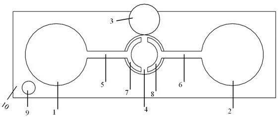
[0033] The first step: Spin-coat photoresist on the upper surface of GaN on the silicon-based GaN wafer, and then use optical lithography to define the pattern of the hole structure on the spin-coated photoresist layer, and define the first active Figures corresponding to the coupling cavity 3, the second active coupling cavity 4, the first pin support 11, the second pin support 12, the first cantilever beam support 13, and the second cantilever beam support 14;

[0034] The second step: use ICP etching technology to etch the nitride layer down to the upper surface of the silicon substrate layer, and then continue to etch downward, and copy the pattern to the silicon, so as to transfer the pattern defined in the first step to the silicon substrate In the gallium nitride layer of the nitride wafer, four disc structures connected by c...

Embodiment 1

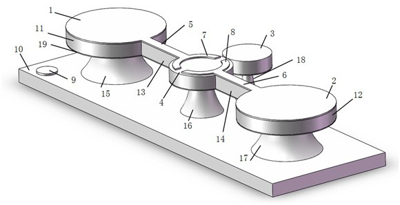
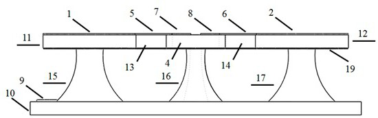
[0043] Using a silicon-based nitride wafer as a carrier, from bottom to top, there are silicon substrate layer, aluminum nitride layer, gallium nitride layer, and left and right ring electrodes and electrode pin holders respectively set on a single gallium nitride microdisk , connected by a cantilever beam structure in the middle. The silicon substrate layer of the microdisk wafer is etched by silicon technology through wet method, and the inside is hollowed out, only the side wall and the bottom tapered column support part are reserved, forming a suspended cavity under the gallium nitride layer. The microdisk is equipped with two cantilever beams that are cut from the gallium nitride layer down to at least the gallium nitride layer, the aluminum nitride layer, and the cavity. Connected with the device, the left half-ring electrode and the right half-ring electrode respectively extend left and right and connect to the middle microdisk. The diameter of the microdisk in the mid...

Embodiment 2

[0045] The electro-optical control method of the gallium nitride microdisk of the present invention uses a silicon-based nitride wafer as a carrier, and sequentially includes a silicon substrate layer, an aluminum nitride layer, a gallium nitride layer, and the left side respectively arranged on a single gallium nitride microdisk from bottom to top Half ring electrode and right half ring electrode. The silicon substrate layer of the microdisk wafer is etched by silicon technology through wet method, and the inside is hollowed out, only the side wall and the bottom tapered column support part are reserved, forming a cavity under the gallium nitride layer. The microdisk is equipped with two cantilever beams that are cut from the gallium nitride layer down to at least the gallium nitride layer, the aluminum nitride layer, and the cavity. Connected with the device, the left half-ring electrode and the right half-ring electrode respectively extend left and right and connect to the ...


PUM

PropertyMeasurementUnit
diameteraaaaaaaaaa
thicknessaaaaaaaaaa
thicknessaaaaaaaaaa

Abstract

The invention discloses an electrically-controlled active coupled cavity laser, which comprises a silicon substrate. A first active coupled cavity, a second active coupled cavity and a silicon substrate electrode are arranged on the silicon substrate; the first active coupled cavity and the second active coupled cavity are fixed on the silicon substrate through silicon columns. aluminum nitride layers are arranged between the bottoms of the first active coupled cavity and the second active coupled cavity and the silicon columns; a first coupled cavity electrode and a second coupled cavity electrode are arranged at the top of the second active coupled cavity; and the first coupled cavity electrode and the second coupled cavity electrode are both of a semicircular structure and are oppositely arranged. Under optical excitation, transverse and longitudinal electric fields are provided for the active cavities through different combined power supply modes of the three electrodes, and regulation and control of a light-emitting mode are achieved.

Description

technical field [0001] The invention belongs to the technical field of visible light, and relates to an electrically regulated active coupled cavity laser. Background technique [0002] GaN-based semiconductor technology has developed rapidly since its birth. Due to its advantages such as high photoelectric conversion efficiency, wide coverage wavelength range, long service life, and direct modulation, it has been widely used in various fields. [0003] Compared with the bulk structure, the microcavity can effectively realize the confinement of the optical field, enhance the interaction between light and matter, and thus improve the performance of the device. Meanwhile, the presence of microcavities can enrich the optical processes in bulk materials. The development of microfabrication technologies such as photolithography and reactive ion etching provides the possibility to design and fabricate GaN optical microcavities. Optoelectronic devices based on GaN microcavities, ...

Claims


Application Information

Patent Timeline
Patent Type & Authority Applications(China)
IPC IPC(8): H01S5/10H01S5/042
CPCH01S5/1021H01S5/1042H01S5/04254
Inventor 秦飞飞王鹏辉刘沣阅朱刚毅
Owner NANJING UNIV OF POSTS & TELECOMM
Why Eureka
Try Eureka