

A micropipe three-dimensional heterojunction device structure and its preparation method and application
A device structure and heterojunction technology, used in semiconductor devices, electrical components, final product manufacturing, etc., can solve the problems of inability to fabricate micro-tubular three-dimensional heterojunction devices, and achieve wide light emission or light receiving directions and low dark current. , the preparation method is simple
- Summary
- Abstract
- Description
- Claims
- Application Information
AI Technical Summary
Problems solved by technology
Method used
Image

Examples
Embodiment 1
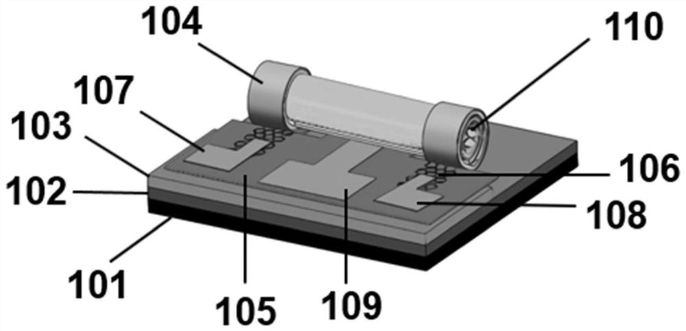
[0061] This embodiment provides a schematic diagram of a three-electrode micropipe three-dimensional heterojunction device structure, as figure 1 shown, the device includes:
[0062] Substrate 101, buffer layer 102, sacrificial layer 103, semiconductor 104, insulating layer 105, two-dimensional material 106, inner wall electrode one 107, inner wall electrode two 108, outer wall electrode 109, micropipe semiconductor / two-dimensional material three-dimensional heterojunction 110. The semiconductor 104 is on the sacrificial layer 103 , and the semiconductor 104 is strained, specifically, it can be a semiconductor compressively strained single layer or a semiconductor strained double layer. The semiconductor 104 and the two-dimensional material 106 are first stacked on the sacrificial layer 103 to form a semiconductor / two-dimensional material planar heterojunction, and further, the sacrificial layer 103 at the bottom is selectively etched away, so that the planar heterojunction i...
Embodiment 2
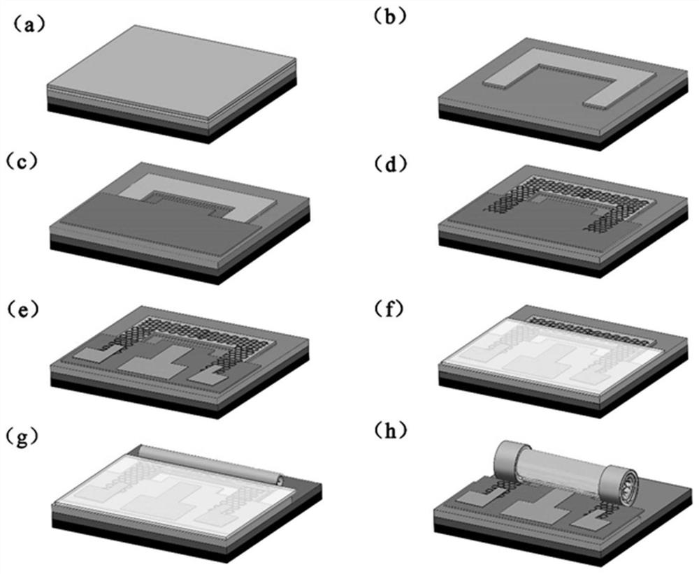
[0066] This embodiment provides a method for preparing a three-electrode microtube semiconductor / two-dimensional material three-dimensional heterojunction device structure, such as figure 2 shown, including steps:
[0067] (a): On the substrate 101, a buffer layer 102, a sacrificial layer 103, and a semiconductor 104 are sequentially deposited to obtain a complete epitaxial structure. Wherein, optionally, the semiconductor 104 is a semiconductor strained double layer composed of a semiconductor compressively strained layer and an unstrained semiconductor top layer;
[0068] (b): U-shaped mesa is formed by photolithography and etching of the epitaxial structure, and the sacrificial layer 103 is exposed at the same time;
[0069] (c): Deposit an insulating layer 105, and photolithography and etch a pattern on the insulating layer 105, so that the insulating layer 105 covers the rear end area of the U-shaped arm on both sides of the U-shaped mesa and the space between the two...
Embodiment 3
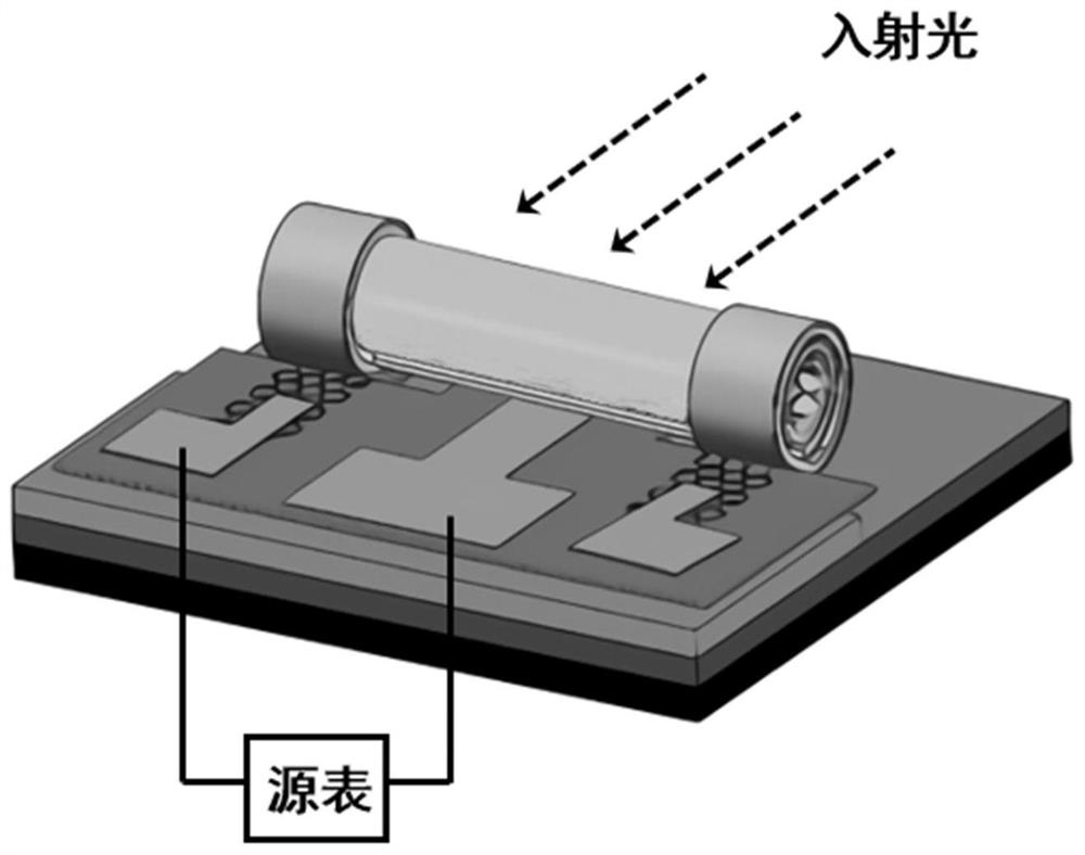
[0076] Such as image 3 Shown, in embodiment 1 of the present invention figure 1 The described three-electrode micropipe three-dimensional heterojunction device can work with two electrodes (an outer wall electrode and any inner wall electrode). Weld electrode leads for the device, optional device packaging, and connect the outer wall electrode and any inner wall electrode to the source meter. At this time, the three-electrode microtubular three-dimensional heterojunction device is a heterojunction photodetector. The current is provided by the source meter (the source meter is also replaced by other current sources or voltage sources). Pass through the microtubular semiconductor / two-dimensional material three-dimensional heterojunction in the radial direction; when the microtubular semiconductor / two-dimensional material three-dimensional heterojunction itself has a photovoltaic effect, no source meter (or external current source, voltage source) is used but only A closed cur...
PUM
| Property | Measurement | Unit |
|---|---|---|
| electrical resistivity | aaaaa | aaaaa |
| thickness | aaaaa | aaaaa |
Abstract
Description
Claims
Application Information