Power factor corrector circuit in interrupted conduction mode and continuous conduction mode
A power factor correction, circuit technology, applied in high-efficiency power electronic conversion, output power conversion devices, DC power input conversion to DC power output, etc., can solve instability, define closed loop dynamic performance is complex, and is not expected frequency etc.
Pending Publication Date: 2020-12-29
NXP BV
0 Cites 0 Cited by
AI-Extracted Technical Summary
Problems solved by technology
To date, the CCM method and the DCM method have not been combined in a way that allows the power factor corrector to operate DCM and CCM during the mains half cycle
Also, loop gain and dynamic behavior are different in CCM applications and DCM applications in power factor correctors, which makes it more complicated to define c...
Abstract
Embodiments of a method and a device are disclosed. A circuit can include a power factor corrector, wherein two or more desired input variables can be defined for the power factor corrector, and a processor that communicates with the power factor corrector, and which selects variables in the power factor corrector with respect to the two or more desired input variables defined for the power factorcorrector. The two or more desired input variables can include a switching frequency and an input current and the variables can include an amount of operation in a conduction mode and at least one ofa primary peak current and a primary conduction interval. The variables in the power factor corrector can be adapted to the two or more desired input variables to allow the power factor corrector tooperate in an operating mode that can include the conduction mode.
Application Domain
Efficient power electronics conversionAc-dc conversion +1
Technology Topic
PhysicsPower factor corrector +8
Image
Examples
- Experimental program(1)
Example Embodiment
[0073]It should be easily understood that the components of the present embodiment as described herein and shown in the drawings can be arranged and designed in a variety of different configurations. Therefore, as shown in the drawings, the following more detailed description of the various embodiments is not intended to limit the scope of the present disclosure, but only represents the various embodiments. Although various aspects of the embodiments are presented in the drawings, unless otherwise noted, the drawings are not necessarily drawn to scale.
[0074]The present invention may be embodied in other specific forms without departing from the spirit or essential characteristics of the present invention. The described embodiments should be considered in all respects only as illustrative and not restrictive. Therefore, the scope of the present invention is indicated by the appended claims rather than this detailed description. All changes that fall within the meaning and scope of equivalents of the claims may be included in the scope of the claims.
[0075]The references to features, advantages, or similar language throughout this specification do not imply that all the features and advantages that can be achieved with the present invention should be or be in any single embodiment of the present invention. On the contrary, language referring to features and advantages should be understood to mean that a particular feature, advantage, or characteristic described in conjunction with the embodiment is included in at least one embodiment of the present invention. Therefore, discussions of features and advantages and similar language throughout this specification may but do not necessarily refer to the same embodiment.
[0076]Furthermore, the described features, advantages, and characteristics of the present invention may be combined in one or more embodiments in any suitable manner. Those skilled in the relevant art will recognize that, in view of the description herein, the present invention may be practiced without one or more of the specific features or advantages of a specific embodiment. In other cases, it may be recognized in certain embodiments that additional features and advantages may not be present in all embodiments of the present invention.
[0077]The reference to "one embodiment", "an embodiment" or similar language throughout this specification means that a particular feature, structure, or characteristic described in conjunction with the indicated embodiment is included in at least one embodiment of the present invention. Therefore, the phrases "in one embodiment", "in an embodiment" and similar language appearing throughout this specification may, but do not necessarily all refer to the same embodiment.
[0078]Several aspects of the disclosed embodiments are presented with reference to various systems, methods, and devices. These systems, methods, and devices are described in the following detailed description, and in the accompanying drawings, various blocks, modules, components, circuits, steps, operations, processes, algorithms, engines, applications, etc. (which may be individually or collectively referred to as "Element") is shown. These elements can be implemented using electronic hardware, computer software, or any combination thereof. Whether such elements are implemented as hardware or software depends on the specific application and design constraints imposed on the entire system.
[0079]The disclosed embodiment relates to a power factor corrector that can be configured to operate under DCM or CCM, where two or more desired input variables can be defined and an algorithm can be implemented that can handle adjusting the power factor corrector The corresponding variables to adapt to the expected input variables. In one embodiment, the two (or more) input variables are preferably a desired operating frequency and a desired input current and the two corresponding variables are preferably an operating frequency and an input current.
[0080]As will be discussed in more detail herein, the disclosed power factor corrector may be configured to operate at least in part in accordance with an algorithm based on estimation of partial derivatives, which may use partial derivatives to solve a set of equations. Such algorithms may additionally involve steps for driving the switching converter unit using the first peak current "Ipeakh", the ratio "a" and the second peak current "Ipeakl" which can be determined according to Ipeak1=F(a,Ipeakh) or operating.
[0081]In addition, the processing unit may receive an error signal including a first error signal and a second error signal, the first error signal is the difference between the desired switching frequency and the measured switching frequency, and the second error signal is the desired average input current The difference with the measured average input current. Then, the processing unit may generate the first peak current "Ipeakh" and the ratio "a" based on the received error signal. It is also possible to implement components that can limit the operating mode to DCM by calculating the frequency of the BCM (=CCM/DCM boundary) and can also limit the desired switching frequency accordingly. In addition, the power factor corrector may be arranged to include components such as a boost converter, a bridgeless power factor corrector or an interleaved boost converter.
[0082]therefore,Figure 7 A flowchart is shown, which depicts the logical operation of the control method 300 of the power factor corrector in which the desired input current (for example, the average current in the switching period) and the desired frequency can be met. inFigure 7 In the embodiment depicted in, these two parameters can be set independently of each other. The desired input current can then be defined using, for example, the multiplier method as discussed in more detail herein.
[0083]Such asFigure 7 As shown, the control signal 282 can be input to the voltage compensation block 286 that can generate the control signal represented by the parameter "k2" to be output by the voltage compensation block 286 to the multiplier "X". It is also possible to input the instantaneous voltage 284 ("Vmains") together with the control signal 282 to the voltage compensation block 286. The operation indicated by the voltage compensation box 286 (ie, the “Vbus” compensation box) may involve voltage compensation, and the result of the voltage compensation may include the output of the “k2” signal 288. Note that the parameter "k2" (also referred to as "K2" in some examples) as used herein relates to the input control level.
[0084]The transition from control to "k2" may involve the mains voltage compensation operation depicted at block 286. The variable "k2" may then be multiplied by the instantaneous "Vmains" voltage 290 as depicted at block 292 to obtain the shape of the PFC for the desired input current ("Idesired") 296. This desired input current "Idesired" can have an appropriate shape to meet the power factor requirement.
[0085]Note that the power factor corrector may also receive as input the desired switching frequency ("Fswitch_desired") as shown at arrow 298 and the mains peak voltage ("Vmainspeak2") as indicated by arrow 294. The output 302 produced is the average value over the half cycle of the mains.Figure 7 Equation 304 shown in can describe the average output current ("Iout_av").
[0086]Note that terms such as "mains, mains power or mains electricity", "mains voltage" and the like as used herein may refer to general AC power supply. This is in the form of electrical power that can be delivered to, for example, homes and businesses, and can be in the form of electrical power that consumers use when plugging home appliances, televisions, lights, etc. into wall sockets. In the United Kingdom and Canada, the term "mains electricity" is usually used, while the United States uses terms such as grid electricity, wall electricity, and household electricity to refer to mains, mains power, and city electricity. Electric voltage or mainselectricity.
[0087]Figure 8 A waveform 320 representing the input current of the power factor corrector operating in DCM (ignoring parasitic ringing effects) is depicted. After reaching the desired current "Ipeakh" during the primary shock, the current can drop back to zero at the end of the secondary shock. Note that inFigure 8 In the waveform 320 shown, the duration of the "primary + secondary" impact can be scaled to a value of 1. Then, the factor "a" can be defined as the ratio of the "primary + secondary" impact to the total cycle time (=1/Fswitch).
[0088]The frequency "Fbcm" (ie BCM frequency) can be defined as the frequency that will occur under the following circumstances: at a given "Ipeakh", the system will be forced to operate in BCM (Boundary Conduction Mode). For a=1, a BCM operation occurs. Now, for a given a, the frequency will be as shown in Equation 1 below:
[0089]
[0090]And the average current in the switching period is equal to:
[0091]
[0092]Based on the equation of switching frequency "Fswitch", this concept can be compared toPicture 9 CCM operation expansion shown,Picture 9 An example waveform 330 of a power factor corrector is depicted, where the same equation for switching frequency can be used for DCM operation and CCM operation. Using the proposed relationship between "Ipeakh", "Ipeakl" and "a", the same equation for switching frequency can be used for DCM operation and CCM operation. For example, if a=0.5, Ipeak1=Ipeakh(0.5) may be required, which can make Fswitch=Fbcm/0.5. For a<1, the following equation can produce CCM:
[0093]Ipeakl=Ipeakh·(1-a) (3)
[0094]
[0095]
[0096]Picture 10 A block diagram of a system 340 including a processor 342 and a power factor corrector 344 is depicted.Picture 10 The system 240 shown in shows a control function in which the signals "a" and "Ipeakh" can be input to the processor 342 (which isPicture 10 Also shown in the "Processing" box). The signal "Ipeakh" may be output to the power factor corrector 344. The control signal “Ipeak1” may be output from the processor 342 and input to the power factor corrector 344. The control signals "a" and "Ipeakh" and "Ipeakl" can be implemented based on Ipeak1=F(a,Ipeakh) (for CCM, according to the above equation (3), or for DCM, according to 0).
[0097]The processor 342 may additionally generate a gate signal for controlling the power factor corrector 344. Such gate signals can be output from the processor 342 and input to the power factor corrector 344, such asPicture 10 Shown. This same gate signal can also be used for the control operation and timing operation of the power factor corrector 344 and for current sensing and for comparing the sensed inductor current with the "Ipeakh" level and the "Ipeakl" level . Based on the timing information of the primary and secondary shocks, the power factor corrector 344 may also send the signal "Tbcm" from the power factor corrector 344 to the processor 342, which indicates the duration of the actual "primary + secondary" shock .
[0098]Based on the "Ipeakl" and "Ipeakh" values, the power factor corrector 344 circuit can control the duration of the primary and secondary shocks of the CCM operation. During DCM operation, "Ipeak1" can be zero. In this case, the processor 342 may use the signal "Tbcm" and the signal "a" to define the duration of the total switching period. Based on the values of "a" and "Tbcm", the processor 342 can perform, for example,Figure 8 The waveform 320 shown in defines the duration of the waiting interval after the end of the secondary shock and before the next primary shock is allowed to start.
[0099]Picture 11 A block diagram of a system 350 for setting appropriate parameters to achieve the desired switching frequency and input current level of the power factor corrector is depicted. That is, another aspect of the disclosed embodiment involves setting appropriate values of "a" and Ipeakh and Ipeak1=F(a,Ipeakh) in order to achieve the desired switching frequency (desired "Fswitch") and input current level (desired "Iin") function.
[0100]therefore,Picture 11 It is shown that the system 350 includes a processing unit 356, a switching converter 358, a calculator unit 360 for calculating the average current in a switching period, a subtraction unit 352 for comparing the desired switching frequency with the actual switching frequency, and a subtraction unit 352 for comparing the desired switching frequency with the actual switching frequency. An embodiment of the subtraction unit 354 that compares the input current with the actual input current. In some example embodiments, the processing unit may be implemented asPicture 10 The processor 342 shown in is a different processor. In other embodiments, the processing unit 356 and the processor 342 may be implemented as part of the same processing device.
[0101]In any case, the processing unit 356 can process a simplified calculation model for the switching converter with Iav_in=F(a, Ipeakh) and Fswitch=f(a, Ipeakh).
[0102]At a certain moment, the switching converter 358 can operate with the values a=a1 and Ipeakh=Ipeakh1. Based on this value, the resulting switching frequency "Fswitch" and the average input current "Iav_in" during the switching period can be tracked and measured. The switching frequency "Fswitch" can be measured directly, for example, by checking the gate signal of the power factor corrector switch. The value of the average input current “Iav_in” may be calculated by the calculator unit 360 based on the primary current sensed over time.
[0103]The switching converter 358 can be driven using a first peak current ("Ipeakh"), a ratio "a", and a second peak current: (Ipeak1)=F(a,Ipeakh). The processing unit 356 may receive two error signals, where the first error signal may constitute the difference between the expected switching frequency and the measured switching frequency, and the second error signal may include the difference between the expected average input current and the measured average input current. The processing unit 356 may generate a first peak current ("Ipeakh") and a ratio "a" based on the received error signal.
[0104]Picture 12 ,13, 14, 15, 16, 17, 18, and 19 depict various equations for calculating the DCM parameters and CCM parameters of the power factor corrector. Based on the calculation model and the operating points at Iin and Fswitch, if the partial effect of changing "a" or Ipeakh (and also changing Ipeakl according to Ipeakl = F(a, Ipeakh)) is known, you can calculate "a" and Ipeak The new value.
[0105]The total effect on the average input current "Iav_in" and the switching frequency "Fswitch" can be achieved by changing the sum of the bias effects of "a" and "Ipeak" and can be determined byPicture 12 The partial derivative indicated by equation 380 shown in. In some cases, it may be necessary to change "a" and "Ipeak" to move the average input current "Iav_in" and the switching frequency "Fswitch" to a desired level within a desired distance. This means that it can be solved fromPicture 12 "Da" and "dIpeakh" of Equation 380 shown in.
[0106]based onPicture 11 Writing the equation in the block diagram of the system 350 shown in, we can getFigure 13 As shown in or asPicture 14 Equation 382 is written in the matrix form indicated by Equation 384 in.
[0107]Such asFigure 15 Equation 386 andFigure 16 As shown in equation 388, a set of equations can be solved in a structured manner. In other words,Figure 15 Equation 386 in can solve for the value "da" and equation 388 can solve for the value "dlpeak". inFigure 17 Here, equation 390 can be the determinant of the system matrix. By replacing the first or second column of the system matrix with the following vector, the following results can be obtained:
[0108]
[0109]Then, you can get the difference asFigure 18with19Two other determinants 392 and 394 are shown. These determinants can be used as numerators to compare with denominators (ie, seeFigure 17 ) Calculate "da" together (ie, seeFigure 15 In equation 386) and "dIpeak" (ie, seeFigure 16 In equation 388).
[0110]Based on this calculation (which can be used to solve asPicture 11 The new value of "a" and "Ipeakh" of the next switching period can be calculated to ensure the switching frequency "Fswitch" and the average input current " Iav_in" is equal to the expected value.
[0111]When correctly calculating the following four partial derivatives
[0112] with
[0113]At this time, the system can converge to the desired operating point with the desired value of the switching frequency "Fswitch" and the average input current "Iav_in" within a switching cycle.
[0114]According to one embodiment, the partial derivative may be calculated based on the equation of the switching converter 358 in conjunction with sensing the desired value of the variable in the equation.
[0115]For a boost converter with input voltage "Vin", output voltage "Vout", mains inductance "Lind" and primary peak current level "Ipeakh", the BCM switching frequency "Fbcm" can be switched as shown in equation (6) "Approximation:
[0116]
[0117]Use this article aboutFigure 8 with9The concept in question can be obtained as the switching frequency "Fswitch" shown in equation (7):
[0118]
[0119]Then, the partial derivative can be easily calculated as shown in the following equations (8) and (9):
[0120]
[0121]as well as
[0122]
[0123]For the average input current, different equations can appear depending on whether the system is operating in DCM or CCM. Under DCM, for example, the average input current in the switching period can be calculated as shown in equation (10):
[0124]
[0125]Under CCM, the average input current in the switching period can be calculated as shown in equation (11):
[0126]
[0127]For BCM operations, in the case of a=1, the two equations can produce the same result:
[0128]
[0129]Then, the partial derivatives of both DCM and CCM can be calculated as shown in equations 13, 14, 15, and 16.
[0130]DCM:
[0131]
[0132]
[0133]CCM:
[0134]
[0135]
[0136]According to Equation 8 and Equation 9, the calculation of partial derivatives may require that "Vin", "Vout" and "Lind" are known. The input voltage "Vin" and the output voltage "Vout" can be directly or indirectly measured and the mains inductance "Lind" can be assumed to be a fixed value known according to the design, and therefore programmed as a constant.
[0137]Picture 20 A flowchart of a method 400 for determining the values of "Ipeakh" and "a" required for every "N" switching cycles is depicted, where "N" may be an integer ≥1. As indicated at block 402, the steps or operations of setting initial values of "a" and "ipeakh" may be implemented. Next, as shown at decision block 404 and block 406, at the beginning of each "Nth" switching period (N can be set to an integer value of at least 1), the calculation procedure can be completed according to the previously discussed equation. The operation of this program is summarized as shown in block 406.
[0138]Optionally, after the processing of the operation shown at block 406, the "a" and "Ipeakh" calculated from the filter pair that processes a part of the old value and a part of the new value may be calculated as shown at block 408 Value is filtered. The resulting values of "a" and "ipeakh" can then be set as output, as depicted at block 410. The operations shown at decision block 404, block 406, etc. can then be repeated.
[0139]Therefore, the method 400 allows the updated calculation to be used shortly after the beginning of the primary shock. If the primary shock is short, the calculations may not be fast enough or more parallel processing may be required, especially considering more circuit area.
[0140]Figure 21 Depicts a graph of voltage and current data versus time (in microseconds) for an example power factor corrector. In some embodiments, the above calculation procedure may be implemented based on the end of the primary shock or the beginning of the secondary shock. This method can provide certain advantages, in which even though the duration of the primary shock may be zero or almost zero, the secondary shock can have the smallest duration (for example, seeFigure 21 420 in the graph). This situation may occur because the switch may be turned on (V(g)) during the primary impact of the power factor corrector, thereby releasing the drain voltage (V(d)). Since there may be parasitic capacitance at the drain node, it may take at least some time to charge the drain node to the level of Vin, and during this interval, current may accumulate in the PFC inductance (I(La)). This means that the secondary shock duration can occur at least during the ringing period, which can allow the algorithm more time to calculate the new "a" value and "Ipeak" value.
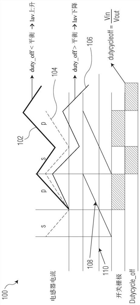
[0141]Figure 22 A schematic diagram 450 of calculation based on the detected average periodic current and frequency is depicted, in which the result of the period "n" with respect to the primary impact and the repetition interval is applied to the period "n+2". It is assumed that the input voltage, output voltage, expected input current, and expected frequency may not change after the start of period "n" and the steady state situation at the start of period "n+2", because the appropriate values of "a" and Ipeak are based on expectations The situation is calculated.
[0142]At the end of period "n+2", the actual frequency and average current can be used based on the new settings initiated at period "n" and new calculations can be made. This means that the minimum repetition interval for updating "a" and "Ipeak" can be every 3 cycles. One advantage of this embodiment is that it can allow calculations to be slower, which in turn can save IC (Integrated Circuit) chip area, because the resulting calculations may need to be presented at the end of the period "n+1".
[0143]The disadvantage of this method may be that there may be three switching cycles between the change in one of the determined variables (for example, Vin, Vout, Fswitch_desired, Iin_desired) and the power factor corrector’s operating point that meets this desired setting. delay. In practice, this means that there is a phase shift between the input current and the input voltage of the PFC. Because the effect is known, the effect can be partially compensated.
[0144]Figure 23 A block diagram of a system 460 for maintaining DCM operation of the PFC is depicted. Note that in some embodiments, CCM prevention can be applied in combination with the previously described features. CCM prevention can be based on calculating the BCM operating frequency based on the actual frequency and the actual value of "a" according to the following equation (16):
[0145]Fbcm=Fswitch·a (16)
[0146]Figure 23 The system 460 shown in may be implemented to maintain the PFC in DCM. As shown in block 462, operations for calculating "Fbcm" may be implemented. The factor "a" can bePicture 11 The output of the processing unit 356 can be combined with the actually measured switching frequency ("Fswitch") as an input and fed toFigure 23 As shown in block 462, this can produce a calculated value of "Fbcm". Then, as indicated at block 464, the value "Fbcm" can be multiplied by a factor "b" that can be slightly less than 1 (eg, 0.95). A factor (such as 0.95) may allow the overall power factor corrector system or power factor corrector circuit to operate in DCM at a frequency slightly lower than the BCM frequency, which may allow the system to use valley switching.
[0147]The calculated value can then be provided to the x input to the "min" operation as shown at block 466, which receives the minimum of the a and y inputs. As a result, as long as the system is operating in DCM (this may be the case where the FBCM is greater than the desired switching frequency "Fswitch_desired"), the desired switching frequency output "Fswitch_desired_out" of the operation shown at block 466 can be equal to the desired switching frequency "Fswitch_desired" ( For example, seePicture 11 ). When the system tends to enter CCM, the desired switching frequency "Fswitch desired_out" may not reach the desired frequency for entering CCM. Then, the system can be restricted to "DCM only" with a margin as set by input "b".
[0148]In addition to standard power factor corrector applications, the disclosed embodiments can be combined with other power factor corrector topologies, such asFigure 24 with25The interleaved power factor corrector or bridgeless boost power factor corrector shown in is used in combination.
[0149]Figure 24 A schematic circuit diagram of the interleaved power factor corrector 480 is depicted. The power factor corrector 480 may include inductors 482 (LB1) And inductor 484 (LB2). Inductor 482 can be coupled to diode 498 (DB1) And transistor 494 (Q1). Inductor 484 can be coupled to transistor 496 (Q2) and diode 500 (DB2). The diode 498 and the diode 500 may be additionally coupled to the capacitor 502. The transistors 494 and 496 may also be connected to the capacitor 502. The power factor corrector 480 may additionally include a diode 486 (D1) and a diode 490 (D4), and a diode 488 (D2) and a diode 492 (D3).
[0150]The diode 486 and the diode 490 may be coupled to the inductor 482 and the inductor 484. The diode 488 and the diode 492 may be connected to the diode 486 and the diode 490, respectively, and may also be connected to each other and to the transistor 494, the transistor 496, and the capacitor 502. Can be in such asFigure 24 The input voltage V at the interface between the diode 486, the diode 488, the diode 490 and the diode 492 shownAC. The output of the power factor corrector 480 can be obtained at the capacitor 502.
[0151]Figure 25 It depicts a bridgeless boost power that can include a diode 516 ("D1") and a diode 518 ("D2") that can be coupled to each other and to a capacitor 528 ("Co") and a resistor 530 ("Ro") A schematic circuit diagram of the factor corrector 510. The capacitor 528 and the resistor 530 may be arranged in parallel with each other in the bridgeless boost power factor corrector circuit 510. The transistor 520 (Q1) may be arranged in parallel with the diode 521, and the transistor 524 (Q2) may be arranged in parallel with the diode 523.
[0152]The diode 516 may be coupled to the transistor 520 and the diode 521, and the diode 518 may be coupled to the transistor 524 and the diode 523. The bridgeless boost power factor corrector 510 may additionally include an inductor 512 ("Lo") that may be connected to the diode 516, the transistor 520, and the diode 521, and may also be connected to the AC voltage source 514 ("AC line"). The diode 518 may be additionally coupled to the transistor 524 and the diode 523, and may also be coupled to the AC voltage source 514. For the topologies of the power factor corrector 480 and the bridgeless boost power factor corrector 510, the inductor current can be sensed in a manner similar to that in the standard power factor corrector, but the disclosed method is implemented to control the power.
[0153]It should be understood that when the input voltage may be close to 0 (such as may occur when approximately equal to the mains zero crossing), the peak current "Ipeak" may become more difficult to set. The reason is that "Ipeak" may become very low and problems such as switching noise and offset may occur. Therefore, a wider implementation of the "Ipeakh" feature can be used to solve the problem of close to the mains zero crossing by replacing "Ipeak" with "Ton".
[0154]When it is close to the zero-crossing point of the utility power, the disclosed power factor corrector can be operated under DCM operation. Then, the power factor corrector switch on time (Ton) can be proportional to the peak current "Ipeak" and inversely proportional to the input voltage (Vin) and can be scaled with the power factor corrector inductor value ("Lind"). Due to this relationship, "Ton" can be quite large and well defined due to the following 1/Vin relationship:
[0155]Therefore, the value of the peak input current "Ipeak" can be set, and the corresponding value of "Ton" can be calculated. The calculated "Ton" value can be used to set the actual Ton for the primary shock.
[0156]Basically, after the secondary shock ends, especially at low input voltages (for example, approximately Vin=50V), the inductor current may become slightly negative, so we can change the "effective" value of "Ton" It is called the part of "Ton" after the inductor current has become positive. In other words, the basic concept is that "Ton" (effective) can be used as a corresponding variable instead of "Ipeak" to set the value of the desired input variable close to the zero-crossing point of the mains and the required "Ton" can be calculated as " Function of Ipeak" value.
[0157]Figure 26 A flowchart of operation is depicted, which shows a method of operating a power factor corrector. As shown at block 602, the process can be initiated. Thereafter, as shown at block 604, two or more desired input variables may be defined for the power factor corrector. Then, as shown at block 606, the corresponding variable in the power factor corrector can be selected with respect to the two or more desired input variables defined for the power factor corrector. The two or more desired input variables may include switching frequency and input current and the corresponding variables may include the amount of operation in DCM or CCM and primary peak current or primary conduction interval. Then, as shown at block 608, the corresponding variable in the power factor corrector may be adjusted according to the two (or more) desired input variables to allow the PFC circuit to operate in DCM or CCM, as previously discussed.
[0158]As previously discussed, the amount of operation under DCM or CCM can be equal to the ratio "a". In addition, the primary peak current can be used as an external corresponding variable approximately equal to the mains zero-crossing area, and "Ton" can be used in an approximately equal to the mains zero-crossing area. In addition, a portion of the "Ton" that may occur positive inductor current ("Ton_effective") can be scaled to "Ipeak" by an adaptively determined factor.
[0159]Although the operations of one or more of the methods in this article are illustrated and described in a specific order, the order of operations of each method can be changed so that some operations can be performed in the reverse order, or that some operations can be at least partially Execute simultaneously with other operations. In another embodiment, instructions or sub-operations of different operations may be implemented in an intermittent and/or alternating manner.
[0160]It should also be noted that at least some of the operations and elements of the methods described herein may be implemented using software instructions stored on a computer-usable storage medium for computer execution. For example, an embodiment of a computer program product includes a computer usable storage medium for storing a computer readable program.
[0161]The computer-usable or computer-readable storage medium may be an electronic, magnetic, optical, electromagnetic, infrared, or semiconductor system (or device or device). Examples of non-transitory computer usable and computer readable storage media include semiconductor or solid state memory, magnetic tape, removable computer disks, random access memory (RAM), read only memory (ROM), rigid magnetic disks, and optical disks. Current examples of optical disks include compact disk read-only memory (CD-ROM), compact disk read/write (CD-R/W), and digital video disk (DVD).
[0162] Alternatively, the embodiments of the present invention and its elements may be implemented entirely in hardware or in an implementation containing hardware elements and software elements. In an embodiment using software, the software may include but is not limited to firmware, resident software, microcode, and the like.
[0163] Although the specific embodiments of the present invention have been described and illustrated, the present invention should not be limited to the specific component forms or arrangements so described and illustrated. The scope of the present invention will be defined by the appended claims and their equivalents.
PUM


Description & Claims & Application Information
We can also present the details of the Description, Claims and Application information to help users get a comprehensive understanding of the technical details of the patent, such as background art, summary of invention, brief description of drawings, description of embodiments, and other original content. On the other hand, users can also determine the specific scope of protection of the technology through the list of claims; as well as understand the changes in the life cycle of the technology with the presentation of the patent timeline. Login to view more.